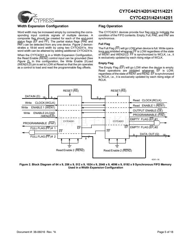
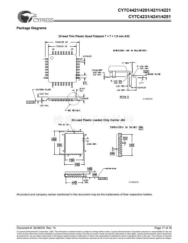
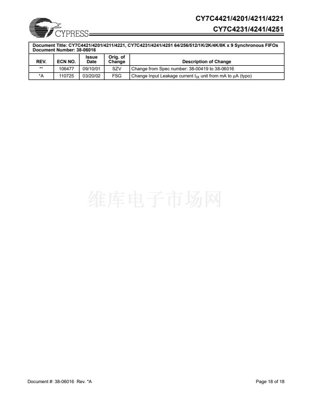
CY7C4421/4201/4211/4221
CY7C4231/4241/4251
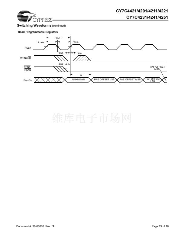
Switching Waveforms
(continued)
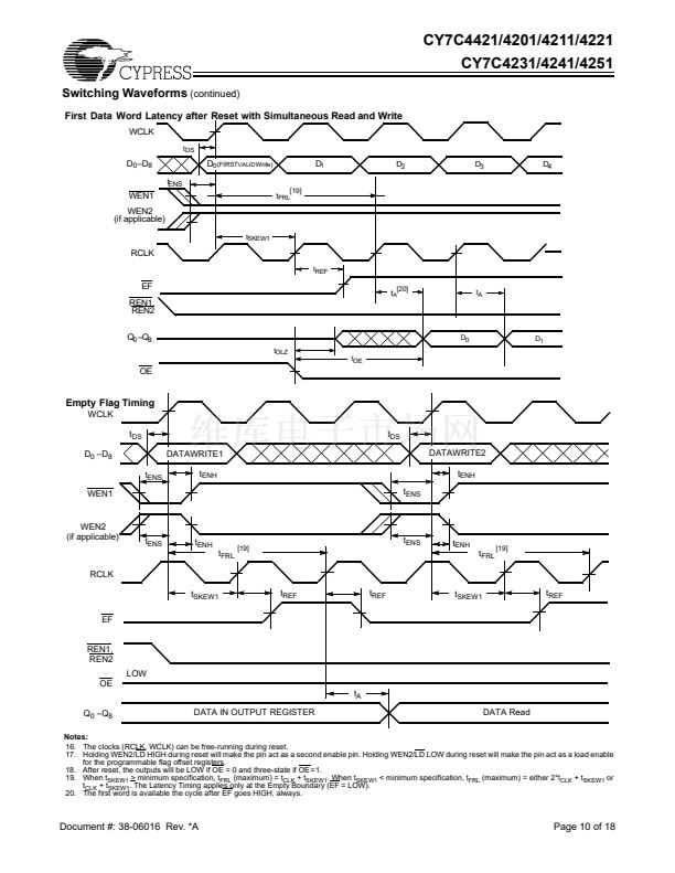
First Data Word Latency after Reset with Simultaneous Read and Write
WCLK
t
DS
D
0
鈥揇
8
t
ENS
D
0 (FIRST
VALID
Write)
[19]
D
1
D
2
D
3
D
4
WEN1
WEN2
(if applicable)
t
SKEW1
t
FRL
RCLK
t
REF
EF
REN1,
REN2
Q
0
鈥換
8
t
OLZ
t
OE
t
A
[20]
t
A
D
0
D
1
OE
Empty Flag Timing
WCLK
t
DS
D
0
鈥揇
8
t
ENS
WEN1
DATAWRITE1
t
ENH
t
ENS
t
DS
DATAWRITE2
t
ENH
WEN2
(if applicable)
t
ENS
t
ENH
t
FRL
[19]
t
ENS
t
ENH
t
FRL
[19]
RCLK
t
SKEW1
EF
REN1,
REN2
LOW
OE
t
A
Q
0
鈥換
8
DATA IN OUTPUT REGISTER
DATA Read
t
REF
t
REF
t
SKEW1
t
REF
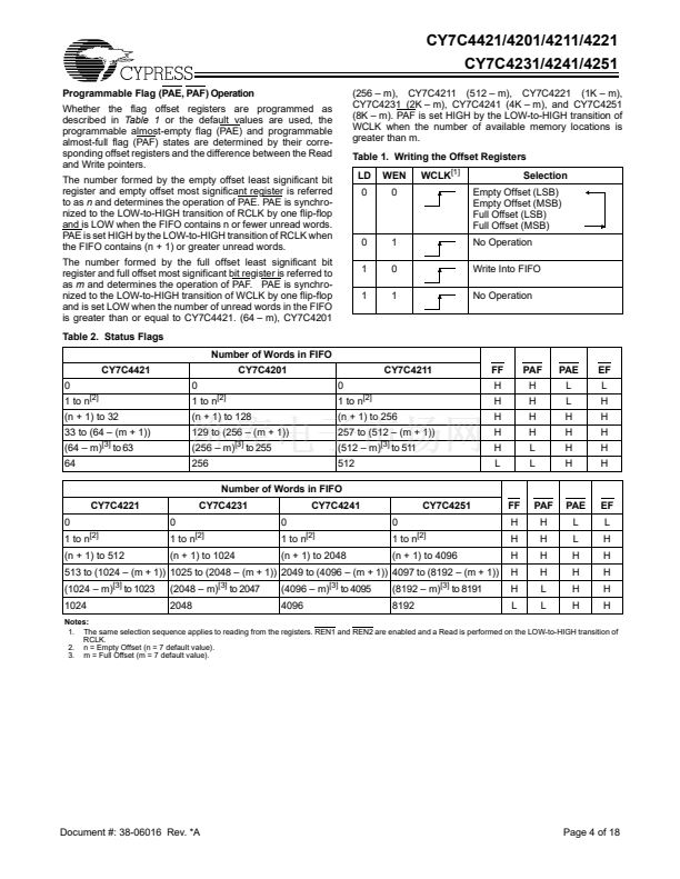
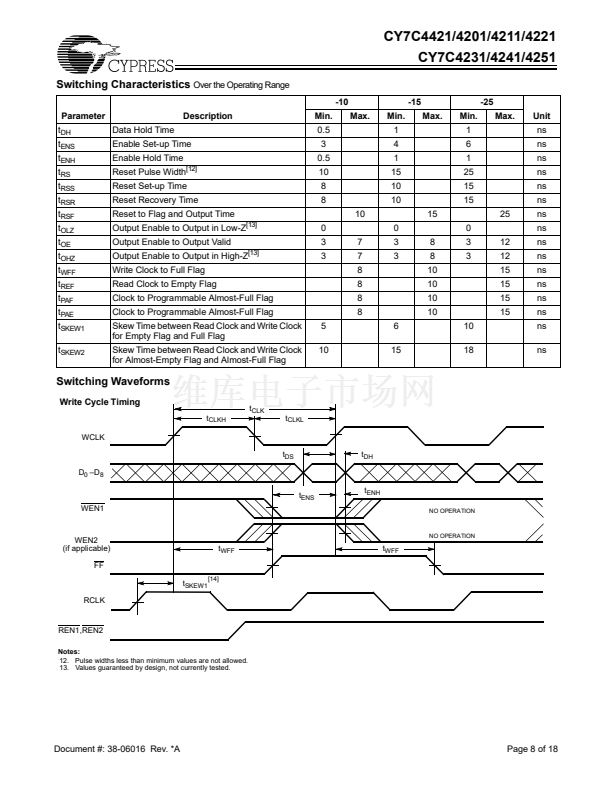
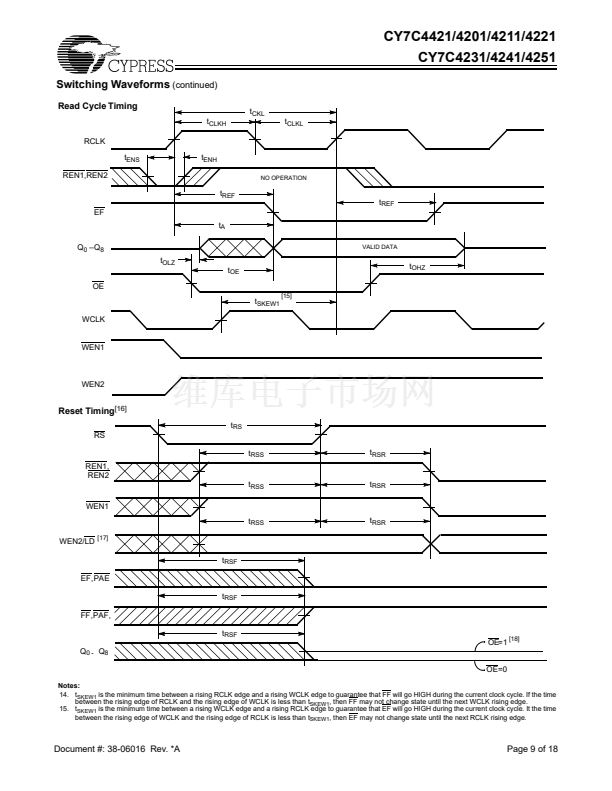
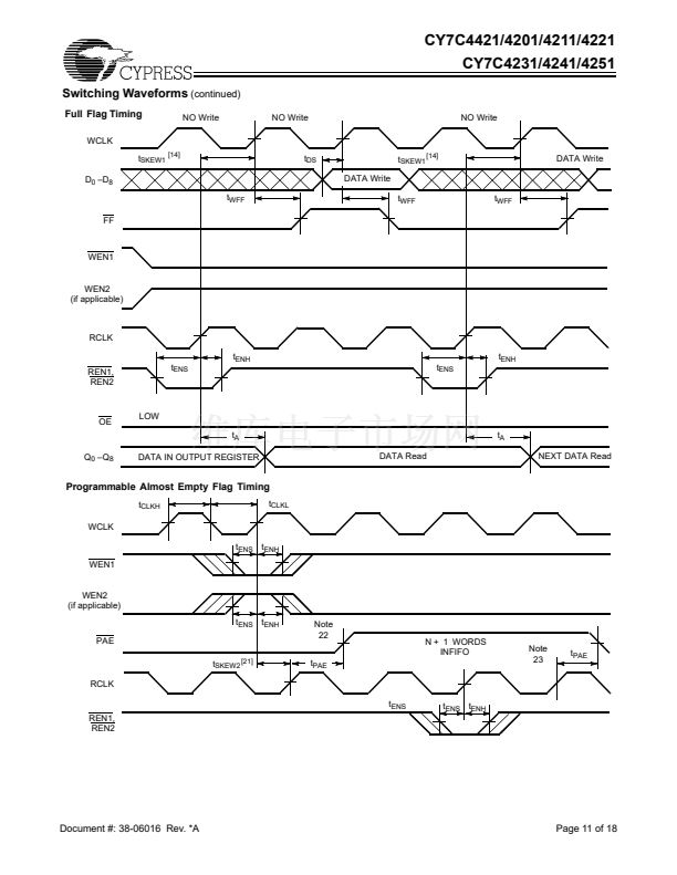
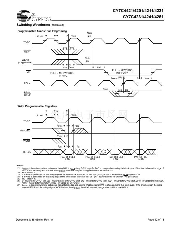
Notes:
16. The clocks (RCLK, WCLK) can be free-running during reset.
17. Holding WEN2/LD HIGH during reset will make the pin act as a second enable pin. Holding WEN2/LD LOW during reset will make the pin act as a load enable
for the programmable flag offset registers.
18. After reset, the outputs will be LOW if OE = 0 and three-state if OE=1.
19. When t
SKEW1
> minimum specification, t
FRL
(maximum) = t
CLK
+ t
SKEW1
. When t
SKEW1
< minimum specification, t
FRL
(maximum) = either 2*t
CLK
+ t
SKEW1
or
t
CLK
+ t
SKEW1
. The Latency Timing applies only at the Empty Boundary (EF = LOW).
20. The first word is available the cycle after EF goes HIGH, always.
Document #: 38-06016 Rev. *A
Page 10 of 18


 1
1
 2
2
 3
3
 4
4
 5
5
 6
6
 7
7
 8
8
 9
9
 10
10
 11
11
 12
12
 13
13
 14
14
 15
15
 16
16
 17
17
 18
18
