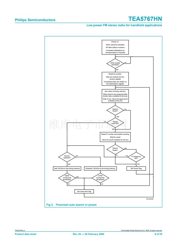
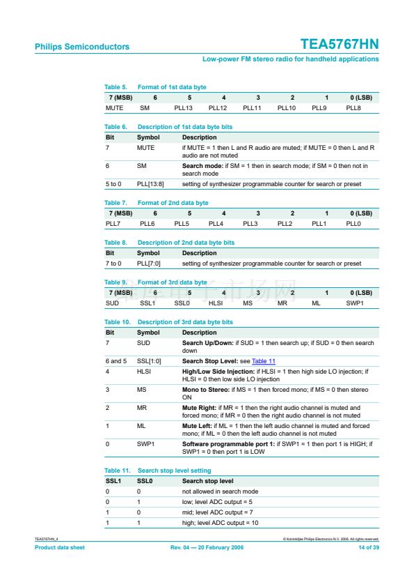
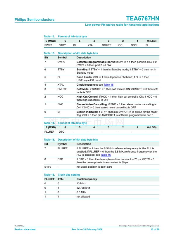
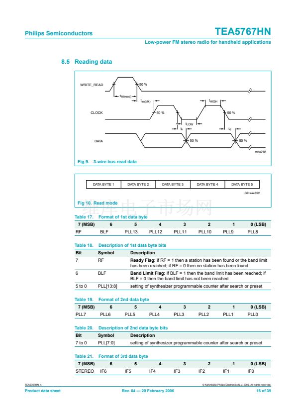
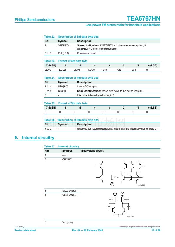
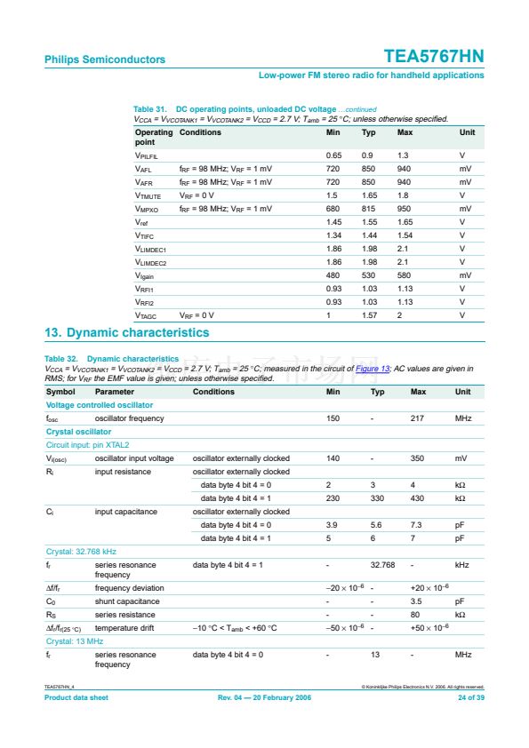
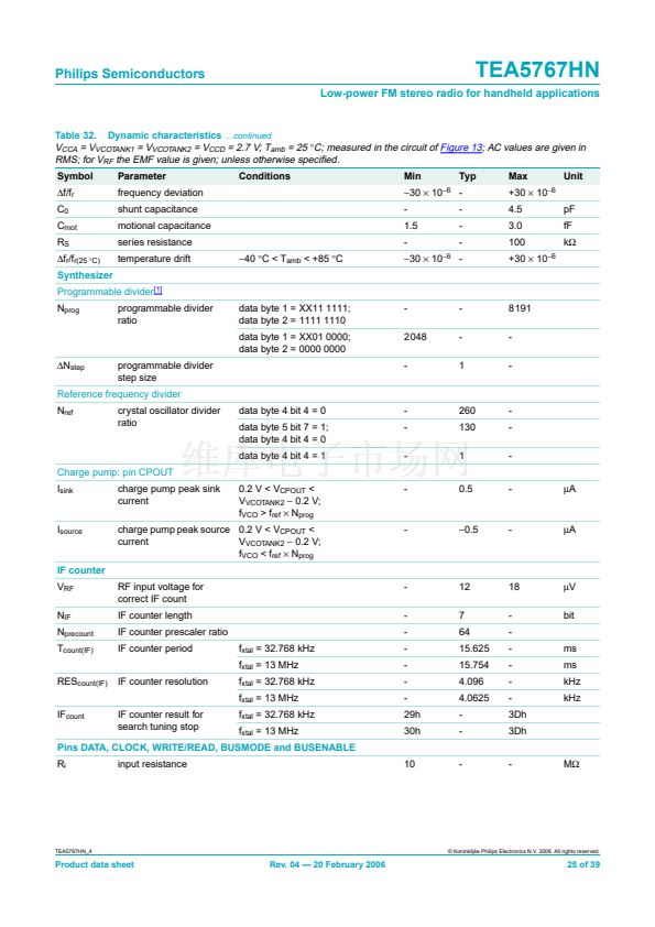
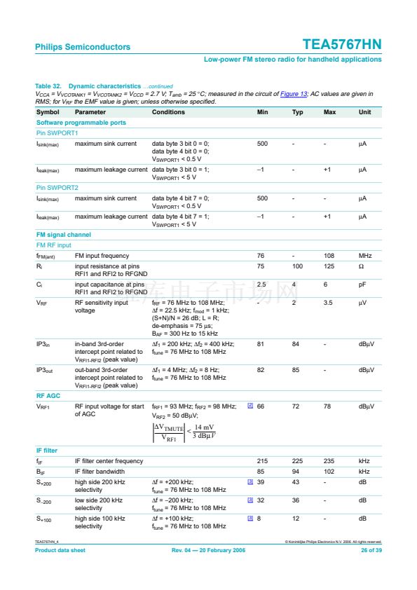
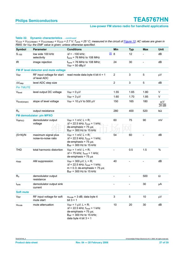
Philips Semiconductors
TEA5767HN
Low-power FM stereo radio for handheld applications
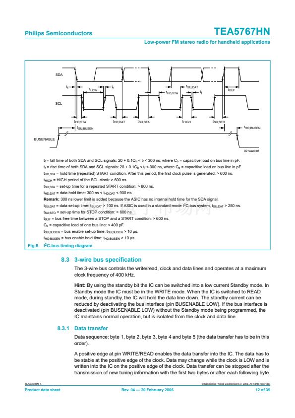
SDA
t
SU;DAT
t
HD;STA
t
f
t
f
t
LOW
t
r
t
BUF
SCL
t
HD;STA
t
SU;BUSEN
BUSENABLE
t
HD;DAT
t
SU;STA
t
HIGH
t
SU;STO
t
HO;BUSEN
001aae349
t
f
= fall time of both SDA and SCL signals: 20 + 0.1C
b
< t
f
< 300 ns, where C
b
= capacitive load on bus line in pF.
t
r
= rise time of both SDA and SCL signals: 20 + 0.1C
b
< t
f
< 300 ns, where C
b
= capacitive load on bus line in pF.
t
HD;STA
= hold time (repeated) START condition. After this period, the 鏗乺st clock pulse is generated: > 600 ns.
t
HIGH
= HIGH period of the SCL clock: > 600 ns.
t
SU;STA
= set-up time for a repeated START condition: > 600 ns.
t
HD;DAT
= data hold time: 300 ns < t
HD;DAT
< 900 ns.
Remark:
300 ns lower limit is added because the ASIC has no internal hold time for the SDA signal.
t
SU;DAT
= data set-up time: t
SU;DAT
> 100 ns. If ASIC is used in a standard mode I
2
C-bus system, t
SU;DAT
> 250 ns.
t
SU;STO
= set-up time for STOP condition: > 600 ns.
t
BUF
= bus free time between a STOP and a START condition: > 600 ns.
C
b
= capacitive load of one bus line: < 400 pF.
t
SU;BUSEN
= bus enable set-up time: t
SU;BUSEN
> 10
碌s.
t
HO;BUSEN
= bus enable hold time: t
HO;BUSEN
> 10
碌s.
Fig 6. I
2
C-bus timing diagram
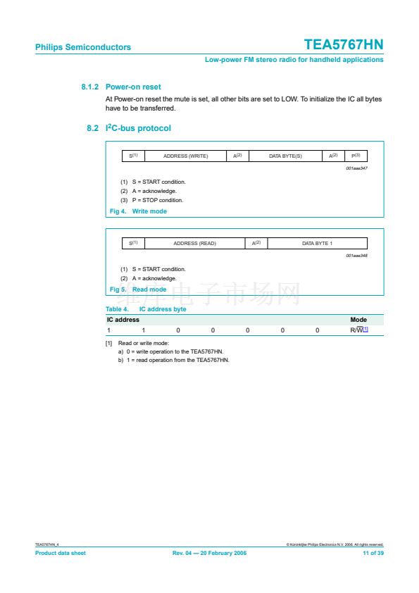
8.3 3-wire bus speci鏗乧ation
The 3-wire bus controls the write/read, clock and data lines and operates at a maximum
clock frequency of 400 kHz.
Hint:
By using the standby bit the IC can be switched into a low current Standby mode. In
Standby mode the IC must be in the WRITE mode. When the IC is switched to READ
mode, during standby, the IC will hold the data line down. The standby current can be
reduced by deactivating the bus interface (pin BUSENABLE LOW). If the bus interface is
deactivated (pin BUSENABLE LOW) without the Standby mode being programmed, the
IC maintains normal operation, but is isolated from the clock and data line.
8.3.1 Data transfer
Data sequence: byte 1, byte 2, byte 3, byte 4 and byte 5 (the data transfer has to be in this
order).
A positive edge at pin WRITE/READ enables the data transfer into the IC. The data has to
be stable at the positive edge of the clock. Data may change while the clock is LOW and is
written into the IC on the positive edge of the clock. Data transfer can be stopped after the
transmission of new tuning information with the 鏗乺st two bytes or after each following byte.
TEA5767HN_4
漏 Koninklijke Philips Electronics N.V. 2006. All rights reserved.
Product data sheet
Rev. 04 鈥?20 February 2006
12 of 39


 1
1
 2
2
 3
3
 4
4
 5
5
 6
6
 7
7
 8
8
 9
9
 10
10
 11
11
 12
12
 13
13
 14
14
 15
15
 16
16
 17
17
 18
18
 19
19
 20
20
 21
21
 22
22
 23
23
 24
24
 25
25
 26
26
 27
27
 28
28
 29
29
 30
30
 31
31
 32
32
 33
33
 34
34
 35
35
 36
36
 37
37
 38
38
 39
39
