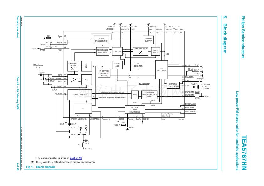
transport direction of the printed-circuit board.
The footprint must incorporate solder thieves at the downstream end.
鈥?/div>
For packages with leads on four sides, the footprint must be placed at a 45擄 angle to
the transport direction of the printed-circuit board. The footprint must incorporate
solder thieves downstream and at the side corners.
During placement and before soldering, the package must be 鏗亁ed with a droplet of
adhesive. The adhesive can be applied by screen printing, pin transfer or syringe
dispensing. The package can be soldered after the adhesive is cured.
Typical dwell time of the leads in the wave ranges from 3 seconds to 4 seconds at 250
擄C
or 265
擄C,
depending on solder material applied, SnPb or Pb-free respectively.
A mildly-activated 鏗倁x will eliminate the need for removal of corrosive residues in most
applications.
18.4 Manual soldering
Fix the component by 鏗乺st soldering two diagonally-opposite end leads. Use a low voltage
(24 V or less) soldering iron applied to the 鏗俛t part of the lead. Contact time must be
limited to 10 seconds at up to 300
擄C.
When using a dedicated tool, all other leads can be soldered in one operation within
2 seconds to 5 seconds between 270
擄C
and 320
擄C.
18.5 Package related soldering information
Table 35.
Package
[1]
BGA, HTSSON..T
[3]
, LBGA, LFBGA, SQFP,
SSOP..T
[3]
, TFBGA, VFBGA, XSON
DHVQFN, HBCC, HBGA, HLQFP, HSO, HSOP,
HSQFP, HSSON, HTQFP, HTSSOP, HVQFN,
HVSON, SMS
PLCC
[5]
, SO, SOJ
LQFP, QFP, TQFP
SSOP, TSSOP, VSO, VSSOP
CWQCCN..L
[8]
, PMFP
[9]
, WQCCN..L
[8]
[1]
[2]
Suitability of surface mount IC packages for wave and re鏗俹w soldering methods
Soldering method
Wave
not suitable
not suitable
[4]
Re鏗俹w
[2]
suitable
suitable
suitable
not recommended
[5][6]
not recommended
[7]
not suitable
suitable
suitable
suitable
not suitable
For more detailed information on the BGA packages refer to the
(LF)BGA Application Note
(AN01026);
order a copy from your Philips Semiconductors sales of鏗乧e.
All surface mount (SMD) packages are moisture sensitive. Depending upon the moisture content, the
maximum temperature (with respect to time) and body size of the package, there is a risk that internal or
external package cracks may occur due to vaporization of the moisture in them (the so called popcorn
effect). For details, refer to the Drypack information in the
Data Handbook IC26; Integrated Circuit
Packages; Section: Packing Methods.
These transparent plastic packages are extremely sensitive to re鏗俹w soldering conditions and must on no
account be processed through more than one soldering cycle or subjected to infrared re鏗俹w soldering with
peak temperature exceeding 217
擄C 鹵
10
擄C
measured in the atmosphere of the re鏗俹w oven. The package
body peak temperature must be kept as low as possible.
[3]
TEA5767HN_4
漏 Koninklijke Philips Electronics N.V. 2006. All rights reserved.
Product data sheet
Rev. 04 鈥?20 February 2006
35 of 39


 1
1
 2
2
 3
3
 4
4
 5
5
 6
6
 7
7
 8
8
 9
9
 10
10
 11
11
 12
12
 13
13
 14
14
 15
15
 16
16
 17
17
 18
18
 19
19
 20
20
 21
21
 22
22
 23
23
 24
24
 25
25
 26
26
 27
27
 28
28
 29
29
 30
30
 31
31
 32
32
 33
33
 34
34
 35
35
 36
36
 37
37
 38
38
 39
39
