錚?/div>
-- ID
VDS=10V
10
7
5
3
2
1.0
7
5
3
2
0.1
7
5
3
2
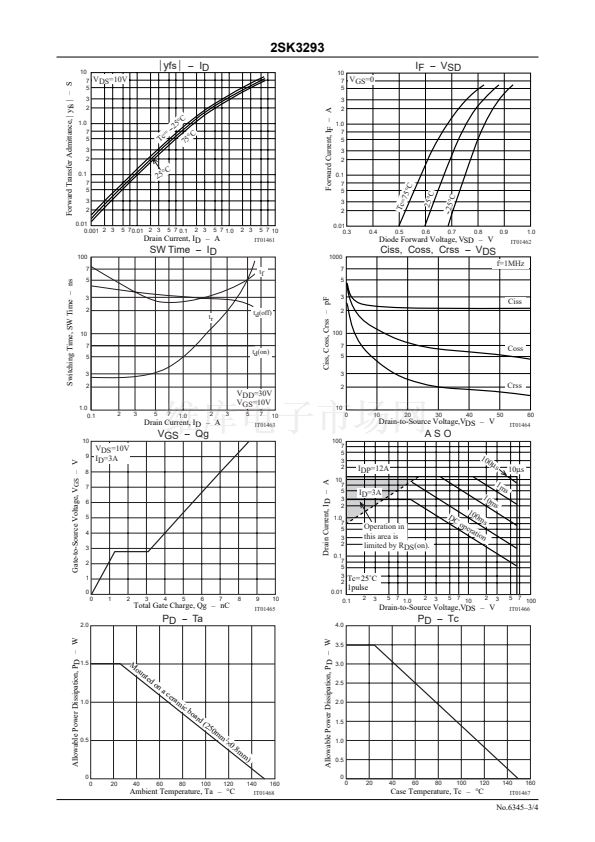
IF -- VSD
VGS=0
=
Tc
--2
C
5
擄
75
擄
C
擄
C
25
Forward Current, IF 鈥?A
75
擄
C
25
擄
C
0.6
0.01
0.3
0.4
0.5
--25
擄
C
0.7
0.8
Tc=
0.9
1.0
IT01462
Drain Current, ID 鈥?A
100
7
Diode Forward Voltage, VSD 鈥?V
SW Time -- ID
tf
Ciss, Coss, Crss -- VDS
f=1MHz
7
5
Switching Time, SW Time 鈥?ns
5
Ciss, Coss, Crss 鈥?pF
3
2
3
2
Ciss
tr
10
7
5
3
2
td(off)
100
7
5
3
td(on)
Coss
1.0
0.1
VDD=30V
VGS=10V
2
3
5
7
1.0
2
3
5
2
Crss
10
0
10
20
30
40
50
60
IT01464
Drain Current, ID 鈥?A
10
9
8
10
IT01463
100
7
5
3
2
7
Drain-to-Source Voltage,VDS 鈥?V
VGS -- Qg
VDS=10V
ID=3A
Drain Current, ID 鈥?A
ASO
10
0
碌
s
Gate-to-Source Voltage, V
GS
鈥?V
IDP=12A
ID=3A
DC
10碌s
7
6
5
4
3
2
1
0
0
1
2
3
4
5
6
7
8
9
10
10
7
5
3
2
1.0
7
5
3
2
0.1
7
5
3
2
1m
s
10
Operation in
this area is
limited by RDS(on).
10
0m
s
op
era
tio
n
ms
Total Gate Charge, Qg 鈥?nC
2.0
0.01
0.1
Tc=25藲C
1pulse
2
3
5 7 1.0
2
3
5 7 10
2
3
IT01465
4.0
Drain-to-Source Voltage,VDS 鈥?V
5 7 100
IT01466
PD -- Ta
Allowable Power Dissipation, PD 鈥?W
PD -- Tc
Allowable Power Dissipation, PD 鈥?W
3.5
3.0
2.5
2.0
1.5
1.0
0.5
0
1.5
M
ou
nte
d
on
a
1.0
ce
ram
ic
b
oa
rd
(2
50
0.5
mm
2
脳
0
.8m
m)
140
160
0
0
20
Ambient Temperature, Ta 鈥?/div>
擄C
40
60
80
100
120
0
20
40
IT01468
Case Temperature, Tc 鈥?/div>
擄C
60
80
100
120
140
160
IT01467
No.6345鈥?/4


 1
1
 2
2
 3
3
 4
4
