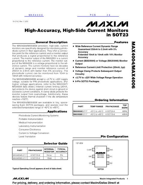
High-Accuracy, High-Side Current Monitors
in SOT23
MAX4004/MAX4006
ABSOLUTE MAXIMUM RATINGS
CLAMP to GND ......................................................-0.3V to +25V
BIAS, REF to GND ..................................................-0.3V to +25V
OUT to GND .........................................-0.3V to (V
CLAMP
+ 0.6V)
Short-Circuit, REF to GND..........................................Continuous
Current into any Pin ..........................................................鹵30mA
Continuous Power Dissipation (T
A
= +70擄C)
6-Pin SOT23 (derate 8.7mW/擄C above +70擄C)............696mW
8-Pin Thin QFN (derate 24.4mW/擄C above +70擄C) ...1951mW
Operating Temperature Range ...........................-40擄C to +85擄C
Junction Temperature ......................................................+150擄C
Storage Temperature Range .............................-65擄C to +150擄C
Lead Temperature (soldering, 10s) .................................+300擄C
Stresses beyond those listed under 鈥淎bsolute Maximum Ratings鈥?may cause permanent damage to the device. These are stress ratings only, and functional
operation of the device at these or any other conditions beyond those indicated in the operational sections of the specifications is not implied. Exposure to
absolute maximum rating conditions for extended periods may affect device reliability.
ELECTRICAL CHARACTERISTICS
(V
BIAS
= 5V, GND = 0V, REF = Open, V
OUT
= 0V (MAX4004), CLAMP = Open, T
A
= -40擄C to +85擄C. Typical values are at T
A
= +25擄C,
unless otherwise noted.) (Note 1)
PARAMETER
Bias Voltage Range
Bias Quiescent Current
Reference Voltage
Thermal Shutdown
Engage Temperature
Trip-Point Temperature
Hysteresis
Input Current Limit
MAX4004
Output Current Noise
SYMBOL
V
BIAS
I
BIAS
V
REF
T
SHDN
T
HYS
I
LIM
CONDITIONS
Inferred from power-supply
rejection test
I
REF
= 250nA
I
REF
= 2.5mA
I
REF
= 2.5mA
REF shorted to GND, junction
temperature rising
REF shorted to GND, junction
temperature falling
V
REF
= V
BIAS
- 5V
f = 0.1Hz to 10Hz
iNOUT
MIN
2.7
TYP
MAX
22
UNITS
V
碌A
mA
V
擄C
擄C
mA
40
3.6
V
BIAS -
1.1
V
BIAS -
0.8
150
5
20
I
REF
= 250nA
I
REF
= 2.5mA
I
REF
= 250nA
I
REF
= 2.5mA
I
REF
= 250nA
I
REF
= 2.5mA
I
REF
= 250nA
I
REF
= 2.5mA
I
REF
= 250nA
I
REF
= 2.5mA
0.3
63
9.2
1240
0.041
0.63
1.3
12.5
50
5
10
1
0 to V
BIAS
- 1.5
0 to V
BIAS
- 0.85
100
4
pA
RMS
f = 0.1Hz to 10kHz
f = 0.1Hz to 10Hz
MAX4006
Output Voltage Noise
e
NOUT
f = 0.1Hz to 10kHz
MAX4004
MAX4006
Output Leakage
Output Voltage Range
V
OUT
REF = open
碌V
RMS
G鈩?/div>
M鈩?/div>
k鈩?/div>
pA
V
Output Resistance
R
OUT
V
BIAS
= 2.7V to 22V, I
REF
= 0 to 1mA,
MAX4004:
鈭咺
OUT
/I
OUT
=
鹵1%,
MAX4006:
鈭哣
OUT
/I
OUT
=
鹵1%
2
_______________________________________________________________________________________


 1
1
 2
2
 3
3
 4
4
 5
5
 6
6
 7
7
 8
8
 9
9
 10
10
 11
11
 12
12
