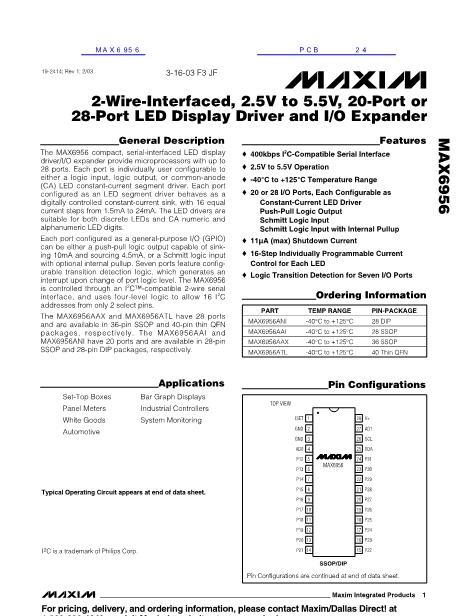
2-Wire-Interfaced, 2.5V to 5.5V, 20-Port or
28-Port LED Display Driver and I/O Expander
MAX6956
ABSOLUTE MAXIMUM RATINGS
Voltage (with Respect to GND)
V+ .............................................................................-0.3V to +6V
SCL, SDA, AD0, AD1................................................-0.3V to +6V
All Other Pins................................................-0.3V to (V+ + 0.3V)
P4鈥揚31 Current ................................................................鹵30mA
GND Current .....................................................................800mA
Continuous Power Dissipation
28-Pin PDIP (derate 20.8mW/擄C above T
A
= +70擄C)1667mW
28-Pin SSOP (derate 9.5mW/擄C above T
A
= +70擄C) ..762mW
36-Pin SSOP (derate 11.8mW/擄C above T
A
= +70擄C) ..941mW
40-Pin QFN (derate 26.3mW/擄C above T
A
= +70擄C) ..2105mW
Operating Temperature Range
(T
MIN
to T
MAX
) ..............................................-40擄C to +125擄C
Junction Temperature ......................................................+150擄C
Storage Temperature Range .............................-65擄C to +150擄C
Lead Temperature (soldering, 10s) .................................+300擄C
Stresses beyond those listed under 鈥淎bsolute Maximum Ratings鈥?may cause permanent damage to the device. These are stress ratings only, and functional
operation of the device at these or any other conditions beyond those indicated in the operational sections of the specifications is not implied. Exposure to
absolute maximum rating conditions for extended periods may affect device reliability.
ELECTRICAL CHARACTERISTICS
(Typical Operating Circuit, V+ = 2.5V to 5.5V, T
A
= T
MIN
to T
MAX
, unless otherwise noted.) (Note 1)
PARAMETER
Operating Supply Voltage
Shutdown Supply Current
SYMBOL
V+
I
SHDN
CONDITIONS
T
A
= +25擄C
T
A
= -40擄C to +85擄C
T
A
= T
MIN
to T
MAX
All ports programmed
as outputs high, no
load, all other inputs at
V+ or GND
All ports programmed
as outputs low, no
load, all other inputs at
V+ or GND
T
A
= +25擄C
T
A
= -40擄C to +85擄C
T
A
= T
MIN
to T
MAX
T
A
= +25擄C
T
A
= -40擄C to +85擄C
T
A
= T
MIN
to T
MAX
110
170
180
MIN
2.5
TYP
5.5
MAX
5.5
8
10
11
230
250
270
210
230
240
135
140
145
0.7
鉁?/div>
V+
0.3
鉁?/div>
V+
GPIO inputs without pullup,
V
PORT
= V+ to GND
V+ = 2.5V
V+ = 5.5V
GPIO outputs, I
SOURCE
= 2mA, T
A
= -40擄C to
+85擄C
GPIO outputs, I
SOURCE
= 1mA, T
A
= T
MIN
to
T
MAX
(Note 2)
V
PORT
= 0.6V
Port configured output low, shorted to V+
-100
12
80
V+ -
0.7
V+ -
0.7
2
2.75
10
11
18
20
鹵1
19
120
0.3
+100
30
180
碌A
碌A
碌A
碌A
UNITS
V
All digital inputs at V+
or GND
Operating Supply Current
I
GPOH
Operating Supply Current
I
GPOL
Operating Supply Current
I
LED
All ports programmed
T
A
= +25擄C
as LED outputs, all LEDs
T
A
= -40擄C to +85擄C
off, no load, all other
inputs at V+ or GND
T
A
= T
MIN
to T
MAX
INPUTS AND OUTPUTS
Logic-High Input Voltage
Port Inputs
Logic-Low Input Voltage
Port Inputs
Input Leakage Current
GPIO Input Internal Pullup to V+
Hysteresis Voltage GPIO Inputs
V
IH
V
IL
I
IH
, I
IL
I
PU
鈭哣
I
V
V
nA
碌A
V
Output High Voltage
V
OH
V
Port Sink Current
Output Short-Circuit Current
I
OL
I
OLSC
mA
mA
2
_______________________________________________________________________________________


 1
1
 2
2
 3
3
 4
4
 5
5
 6
6
 7
7
 8
8
 9
9
 10
10
 11
11
 12
12
 13
13
 14
14
 15
15
 16
16
 17
17
 18
18
 19
19
 20
20
 21
21
 22
22
 23
23
 24
24
 25
25
 26
26
 27
27
