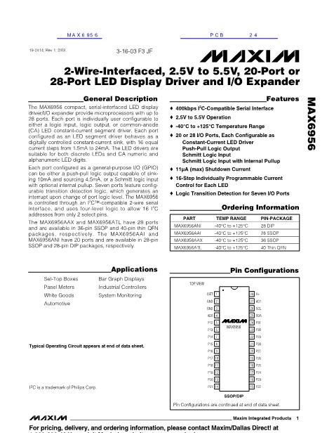
2-Wire-Interfaced, 2.5V to 5.5V, 20-Port or
28-Port LED Display Driver and I/O Expander
MAX6956
Table 1. Port Configuration Map
REGISTER
Port Configuration for P7, P6, P5, P4
Port Configuration for P11, P10, P9, P8
Port Configuration for P15, P14, P13, P12
Port Configuration for P19, P18, P17, P16
Port Configuration for P23, P22, P21, P20
Port Configuration for P27, P26, P25, P24
Port Configuration for P31, P30, P29, P28
ADDRESS
CODE (HEX)
0x09
0x0A
0x0B
0x0C
0x0D
0x0E
0x0F
REGISTER DATA
D7
P7
P11
P15
P19
P23
P27
P31
D6
D5
P6
P10
P14
P18
P22
P26
P30
D4
D3
P5
P9
P13
P17
P21
P25
P29
D2
D1
P4
P8
P12
P16
P20
P24
P28
D0
Table 2. Port Configuration Matrix
MODE
FUNCTION
PORT
REGISTER
(0x20鈥?x5F)
Register bit = 0
Output
LED Segment Driver
Register bit = 1
Register bit = 0
Register bit = 1
Register bit =
input logic level
PIN BEHAVIOR
ADDRESS
CODE (HEX)
PORT
CONFIGURATION
BIT PAIR
UPPER
High impedance
Open-drain current sink, with sink
current (up to 24mA) determined
by the appropriate current register
Active-low logic output
Active-high logic output
Schmitt logic input
Schmitt logic input with pullup
0x09 to 0x0F
0
0
LOWER
Output
Input
Input
GPIO Output
GPIO Input
Without Pullup
GPIO Input with Pullup
0x09 to 0x0F
0x09 to 0x0F
0x09 to 0x0F
0
1
1
1
0
1
Note:
The logic is inverted between the two output modes; a high makes the output go low in LED segment driver mode (0x00) to
turn that segment on; in GPIO output mode (0x01), a high makes the output go high.
simplify access to displays that overlap two MAX6956s,
the MAX6956 provides four virtual ports, P0 through P3.
To update an overlapping digit, send the same code
twice as an eight-port write, once to P28 through P35 of
the first driver, and again to P0 through P7 of the sec-
ond driver. The first driver ignores the last 4 bits and
the second driver ignores the first 4 bits.
Two addressing methods are available. Any single port
(bit) can be written (set/cleared) at once; or, any
sequence of eight ports can be written (set/cleared) in
any combination at once. There are no boundaries; it is
equally acceptable to write P0 through P7, P1 through
P8, or P31 through P38 (P32 through P38 are nonexis-
tent, so the instructions to these bits are ignored).
Using 8-bit control, a seven-segment digit with a deci-
mal point can be updated in a single byte-write, a 14-
6
segment digit with DP can be updated in two byte-
writes, and 16-segment digits with DP can be updated
in two byte-writes plus a bit write. Also, discrete LEDs
and GPIO port bits can be lit and controlled individually
without affecting other ports.
Shutdown
When the MAX6956 is in shutdown mode, all ports are
forced to inputs (which an be read), and the pullup cur-
rent sources are turned off. Data in the port and control
registers remain unaltered, so port configuration and
output levels are restored when the MAX6956 is taken
out of shutdown. The display driver can still be pro-
grammed while in shutdown mode. For minimum sup-
ply current in shutdown mode, logic inputs should be at
GND or V+ potential. Shutdown mode is exited by set-
ting the S bit in the configuration register (Table 8).
_______________________________________________________________________________________


 1
1
 2
2
 3
3
 4
4
 5
5
 6
6
 7
7
 8
8
 9
9
 10
10
 11
11
 12
12
 13
13
 14
14
 15
15
 16
16
 17
17
 18
18
 19
19
 20
20
 21
21
 22
22
 23
23
 24
24
 25
25
 26
26
 27
27
