Serially Interfaced, +2.7V to +5.5V,
5- and 8-Digit LED Display Drivers
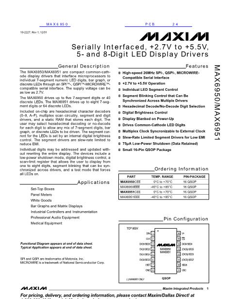
MAX6950/MAX6951
Table 5. Configuration Register Format
MODE
Configuration register
ADDRESS
CODE (HEX)
0x04
REGISTER DATA
D7
X
D6
X
D5
R
D4
T
D3
E
D2
B
D1
0
D0
S
Table 6. Shutdown Control (S Data Bit D0) Format
MODE
Shutdown
Normal operation
ADDRESS
CODE (HEX)
0x04
0x04
REGISTER DATA
D7
X
X
D6
X
X
D5
R
R
D4
T
T
D3
E
E
D2
B
B
D1
0
0
D0
0
1
Table 7. Blink Rate Selection (B Data Bit D2) Format
MODE
Slow-blinking segments
blink on for 1s, off for 1s
with f
OSC
= 4MHz
Fast-blinking segments
blink on for 0.5s, off for
0.5s with f
OSC
= 4MHz
ADDRESS
CODE (HEX)
REGISTER DATA
D7
X
D6
X
D5
R
D4
T
D3
E
D2
0
D1
0
D0
S
0x04
0x04
X
X
R
T
E
1
0
S
Table 8. Global Blink Enable/Disable (E Data Bit D3) Format
MODE
Blink function is
disabled
Blink function is
enabled
ADDRESS
CODE (HEX)
0x04
0x04
REGISTER DATA
D7
X
X
D6
X
X
D5
R
R
D4
T
T
D3
0
1
D2
B
B
D1
0
0
D0
S
S
Table 9. Global Blink Timing Synchronization (T Data Bit D4) Format
MODE
Blink timing counters
are unaffected
Blink timing counters
are cleared on the
rising edge of
CS
ADDRESS
CODE (HEX)
0x04
REGISTER DATA
D7
X
D6
X
D5
R
D4
0
D3
E
D2
B
D1
0
D0
S
0x04
X
X
R
1
E
B
0
S
Each LED digit is represented by 2 bytes of memory, 1
byte in plane P0 and the other in plane P1. Each LED
digit鈥檚 segment is represented by 2 bits of memory, 1
bit from the appropriate byte in each plane. The digit
10
registers are mapped so that a digit鈥檚 data can be
updated in plane P0, or plane P1, or both planes at the
same time (Table 3).
______________________________________________________________________________________


 1
1
 2
2
 3
3
 4
4
 5
5
 6
6
 7
7
 8
8
 9
9
 10
10
 11
11
 12
12
 13
13
 14
14
 15
15
 16
16
 17
17
 18
18
 19
19
