Serially Interfaced, +2.7V to +5.5V,
5- and 8-Digit LED Display Drivers
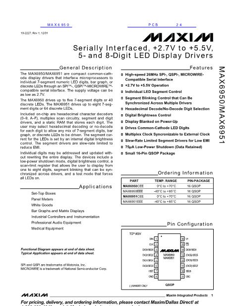
MAX6950/MAX6951
Table 13. Intensity Register Format
DUTY CYCLE
1/16 (min on)
2/16
3/16
4/16
5/16
6/16
7/16
8/16
9/16
10/16
11/16
12/16
13/16
14/16
15/16
15/16 (max on)
TYPICAL SEGMENT
CURRENT (mA)
2.5
5
7.5
10
12.5
15
17.5
20
22.5
25
27.5
30
32.5
35
37.5
37.5
ADDRESS
CODE (HEX)
0x02
0x02
0x02
0x02
0x02
0x02
0x02
0x02
0x02
0x02
0x02
0x02
0x02
0x02
0x02
0x02
D7
X
X
X
X
X
X
X
X
X
X
X
X
X
X
X
X
D6
X
X
X
X
X
X
X
X
X
X
X
X
X
X
X
X
D5
X
X
X
X
X
X
X
X
X
X
X
X
X
X
X
X
D4
X
X
X
X
X
X
X
X
X
X
X
X
X
X
X
X
D3
0
0
0
0
0
0
0
0
1
1
1
1
1
1
1
1
D2
0
0
0
0
1
1
1
1
0
0
0
0
1
1
1
1
D1
0
0
1
1
0
0
1
1
0
0
1
1
0
0
1
1
D0
0
1
0
1
0
1
0
1
0
1
0
1
0
1
0
1
HEX
CODE
0xX0
0xX1
0xX2
0xX3
0xX4
0xX5
0xX6
0xX7
0xX8
0xX9
0xXA
0xXB
0xXC
0xXD
0xXE
0xXF
The allowed range of the frequency at the OSC pin, f
OSC
,
is 1MHz to 8MHz, which allows the blink frequency to be
adjusted over a wide range. The internal oscillator may
be accurate enough for many applications using a single
device. If an exact or synchronized blink rate is required,
then OSC should be driven by an external clock.
The display scan rate (defined in the
Electrical
Characteristics
table) is calculated by dividing f
OSC
by
4000 for the MAX6950 (scanning a full five digits), or by
6400 for the MAX6951 (scanning a full eight digits). The
display scan rate is the refresh rate for all the digits of the
display. With f
OSC
at 4MHz, each display digit is enabled
for 200碌s.
There is a fail-safe circuit in the MAX6950/MAX6951 to
ensure the display multiplexing works if the OSC is con-
figured incorrectly. This ensures that the driver cannot
remain stuck on a single digit, forcing a peak current con-
tinuously through segments. The fail-safe circuit detects
that f
OSC
is too slow, and generates extra clock transi-
tions to guarantee a minimum effective clock of typically
75.5kHz. The scan rate for eight digits is about 11Hz in
fail-safe mode, and appears to flicker to most observers.
A flickering display is a good indication that there is a
problem with the multiplex clock. The clock failure detec-
tion works regardless of the clock source being the inter-
nal RC oscillator or external clock drive.
The RC oscillator uses an external resistor R
SET
(which
also sets the peak segment current) and an external
capacitor C
SET
to set the oscillator frequency. The rec-
ommended values of R
SET
and C
SET
set the oscillator at
4MHz, which makes the slow and fast blink frequency
0.5Hz and 1Hz, respectively.
Synchronization of Blinking Across
Multiple MAX6950/MAX6951 Drivers
The OSC inputs of multiple MAX6950/MAX6951 drivers
can be connected together to an external clock to make
the devices blink at the same frequency. Segment blink-
ing may be synchronized across multiple MAX6950/
MAX6951s so that all drivers blink not only at the same
frequency, but also in phase. When the control register is
written with the T bit set (Table 9), the OSC divider chain
is cleared and the display multiplexing sequence reset.
To synchronize several drivers, it is necessary to write
this register in all drivers at the same time. In practice,
adequate synchronization can be achieved by writing to
multiple drivers in quick succession.
When the global blink timing synchronization bit is set,
the multiplexing and blink counter is cleared on the ris-
ing edge of
CS.
By setting the T bit in multiple
MAX6950/MAX6951s at the same time (or in quick suc-
cession), the blink timing can be synchronized across
all the devices. Note that the display multiplexing
12
______________________________________________________________________________________


 1
1
 2
2
 3
3
 4
4
 5
5
 6
6
 7
7
 8
8
 9
9
 10
10
 11
11
 12
12
 13
13
 14
14
 15
15
 16
16
 17
17
 18
18
 19
19
