50鈩?/div>
OUT-
Figure 2. CML Input Buffer
Figure 3. CML Output Buffer
Signal Detect with Standby Mode
Signal activity is detected on channel 1 only. When the
peak-to-peak differential voltage at IN1鹵 is less than
30mVp-p, the TTL output SDET goes low. When the
peak-to-peak differential voltage becomes greater than
100mVp-p, SDET is asserted high. SDET can be used
to automatically force the equalizer into standby mode
by connecting SDET directly to the EN input. When not
used, SDET should not be connected.
The signal-detect function continues to operate while
the part is in standby mode. While connected to the EN
pin, the signal detect can 鈥渨ake up鈥?the part and
resume normal operation.
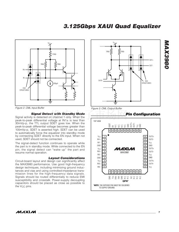
TOP VIEW
SDET
Pin Configuration
N.C.
N.C.
N.C.
GND
OUT1+
OUT1-
41
40
39
38
37
36
44
43
42
35
34
V
CC
GND
EN
N.C.
V
CC
IN1+
IN1-
GND
V
CC
IN2+
IN2-
GND
V
CC
IN3+
IN3-
1
2
3
4
5
6
7
8
9
10
11
12
13
14
15
16
17
18
19
20
21
22
33
32
31
30
29
28
27
26
25
24
23
OUT2+
OUT2-
V
CC
GND
OUT3+
OUT3-
V
CC
GND
OUT4+
OUT4-
V
CC
MAX3980
Layout Considerations
Circuit-board layout and design can significantly affect
the MAX3980 performance. Use good high-frequency
design techniques, including minimizing ground induc-
tances and vias and using controlled-impedance trans-
mission lines for the high-frequency data signals.
Signals should be routed differentially to reduce EMI
susceptibility and crosstalk. Power-supply decoupling
capacitors should be placed as close as possible to
the V
CC
pins.
*NOTE: THE EXPOSED PAD MUST BE SOLDERED
TO SUPPLY GROUND.
_______________________________________________________________________________________
V
CC
IN4+
IN4-
GND
N.C.
N.C.
GND
QFN*
N.C.
N.C.
N.C.
N.C.
7


 1
1
 2
2
 3
3
 4
4
 5
5
 6
6
 7
7
 8
8
 9
9
