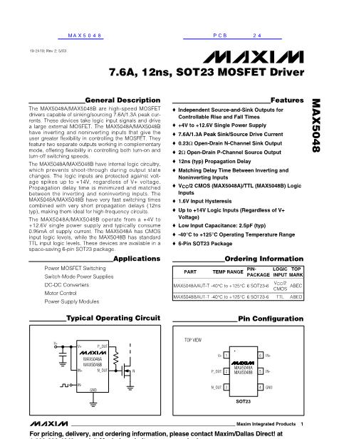
7.6A, 12ns, SOT23 MOSFET Driver
MAX5048
Pin Description
PIN
1
2
3
4
5
6
NAME
V+
P_OUT
N_OUT
GND
IN-
IN+
FUNCTION
Power Supply. Bypass to GND with a
0.1碌F ceramic capacitor.
P-Channel Open-Drain Output. Sources
current for MOSFET turn on.
N-Channel Open-Drain Output. Sinks
current for MOSFET turn off.
Ground
Inverting Logic Input Terminal. Connect
to GND when not used.
Noninverting Logic Input Terminal.
Connect to V+ when not used.
Undervoltage Lockout (UVLO)
When V+ is below the UVLO threshold, the N-channel
is ON and the P-channel is OFF, independent of the
state of the inputs. The UVLO is typically 3.6V with
400mV typical hysteresis to avoid chattering.
Driver Outputs
The MAX5048A/MAX5048B provide two separate out-
puts. One is an open-drain P-channel, the other an
open-drain N-channel. They have distinct current sourc-
ing/sinking capabilities to independently control the rise
and fall times of the MOSFET gate. Add a resistor in
series with P_OUT/N_OUT to slow the corresponding
rise/fall time of the MOSFET gate.
Applications Information
Supply Bypassing, Device Grounding,
and Placement
Ample supply bypassing and device grounding are
extremely important because when large external
capacitive loads are driven, the peak current at the V+
pin can approach 1.3A, while at the GND pin the peak
current can approach 7.6A. V
CC
drops and ground
shifts are forms of negative feedback for inverters and, if
excessive, can cause multiple switching when the IN-
input is used and the input slew rate is low. The device
driving the input should be referenced to the
MAX5048A/MAX5048B GND pin especially when the IN-
input is used. Ground shifts due to insufficient device
grounding may disturb other circuits sharing the same
AC ground return path. Any series inductance in the V+,
P_OUT, N_OUT and/or GND paths can cause oscilla-
tions due to the very high di/dt that results when the
MAX5048A/MAX5048B are switched with any capacitive
load. A 0.1碌F or larger value ceramic capacitor is rec-
ommended bypassing V+ to GND and placed as close
to the pins as possible. When driving very large loads
(e.g., 10nF) at minimum rise time, 10碌F or more of paral-
lel storage capacitance is recommended. A ground
plane is highly recommended to minimize ground return
resistance and series inductance. Care should be taken
to place the MAX5048A/MAX5048B as close as possi-
ble to the external MOSFET being driven to further mini-
mize board inductance and AC path resistance.
Detailed Description
Logic Inputs
The MAX5048A/MAX5048Bs鈥?logic inputs are protected
against voltage spikes up to +14V, regardless of the V+
voltage. The low 2.5pF input capacitance of the inputs
reduces loading and increases switching speed. These
devices have two inputs that give the user greater flexi-
bility in controlling the MOSFET. Table 1 shows all pos-
sible input combinations.
The difference between the MAX5048A and the
MAX5048B is the input threshold voltage. The
MAX5048A has V
CC
/2 CMOS logic-level thresholds,
while the MAX5048B has TTL logic-level thresholds (see
the
Electrical Characteristics).
For V+ above 5.5V, V
IH
(typ) = 0.5x(V+) + 0.8V and V
IL
(typ) = 0.5x(V+) - 0.8V.
As V+ is reduced from 5.5V to 4V, V
IH
and V
IL
gradually
approach V
IH
(typ) = 0.5x(V+) + 0.65V and V
IL
(typ) =
0.5x(V+) - 0.65V. Connect IN+ to V+ or IN- to GND
when not used. Alternatively, the unused input can be
used as an ON/OFF pin (see Table 1).
Table 1. Truth Table
IN+
L
L
H
H
IN-
L
H
L
H
P-CHANNEL
OFF
OFF
ON
OFF
N-CHANNEL
ON
ON
OFF
ON
Power Dissipation
Power dissipation of the MAX5048A/MAX5048B con-
sists of three components, caused by the quiescent
current, capacitive charge and discharge of internal
nodes, and the output current (either capacitive or
resistive load). The sum of these components must be
kept below the maximum power-dissipation limit.
L = Logic low
H = Logic high
6
_______________________________________________________________________________________


 1
1
 2
2
 3
3
 4
4
 5
5
 6
6
 7
7
 8
8
 9
9
