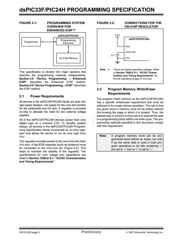
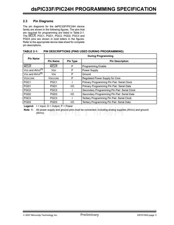
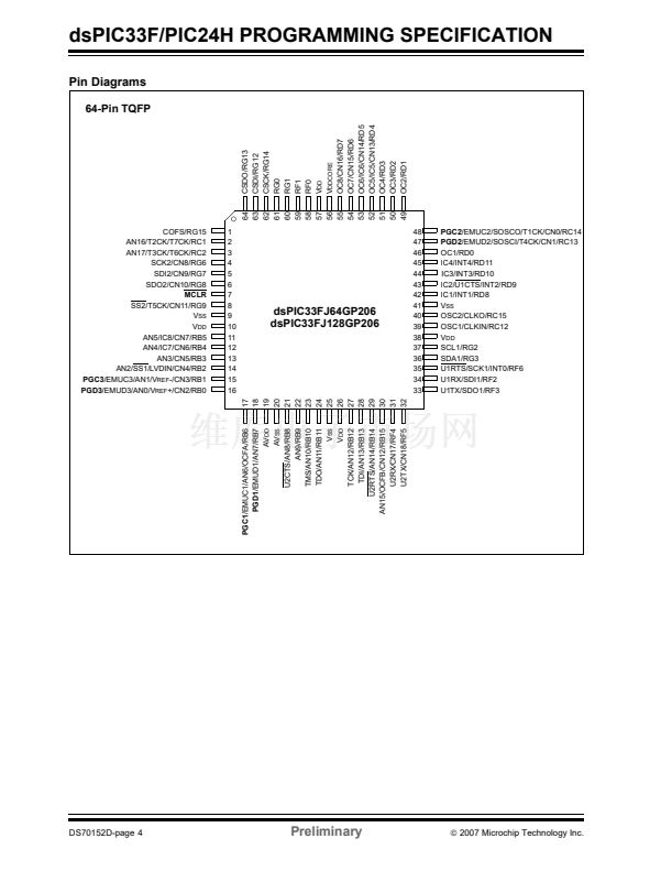
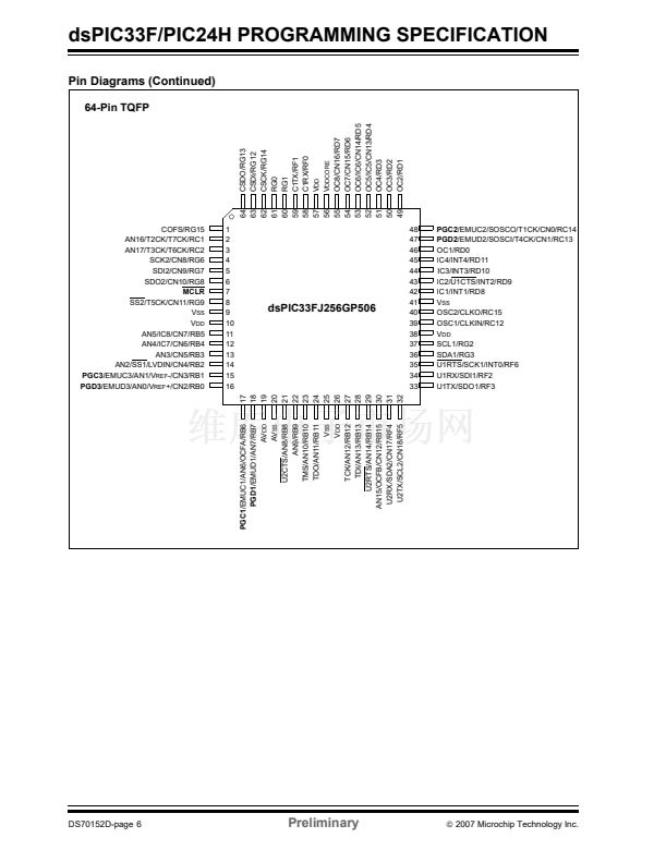
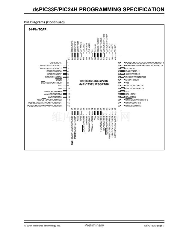
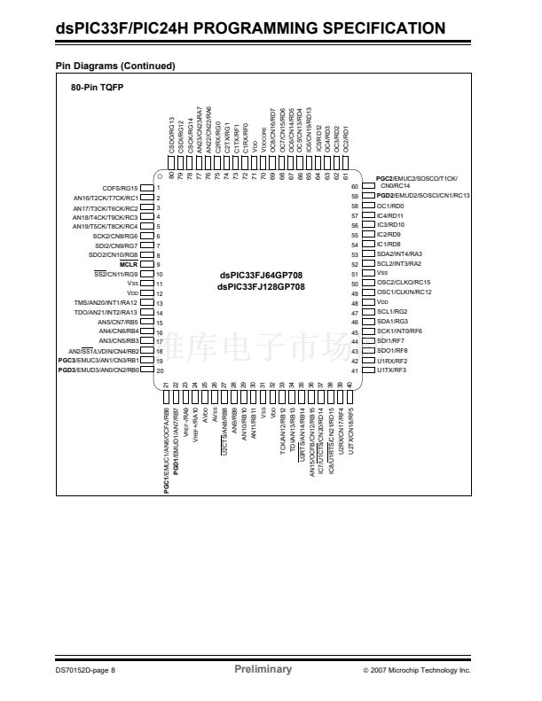
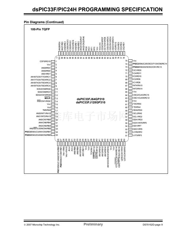
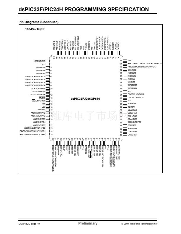
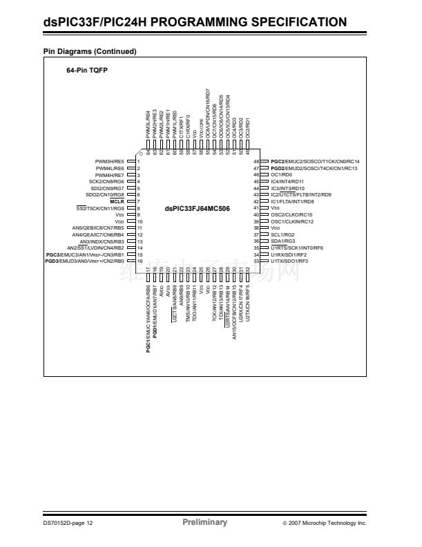
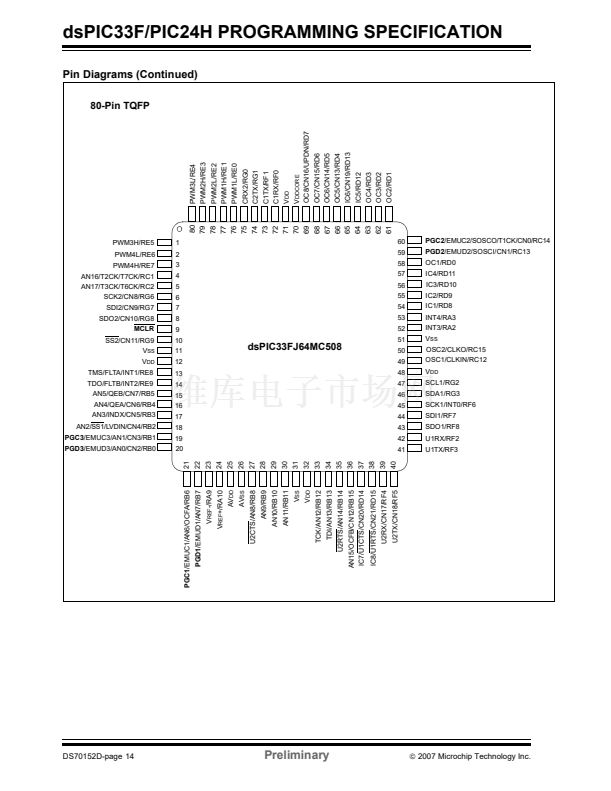
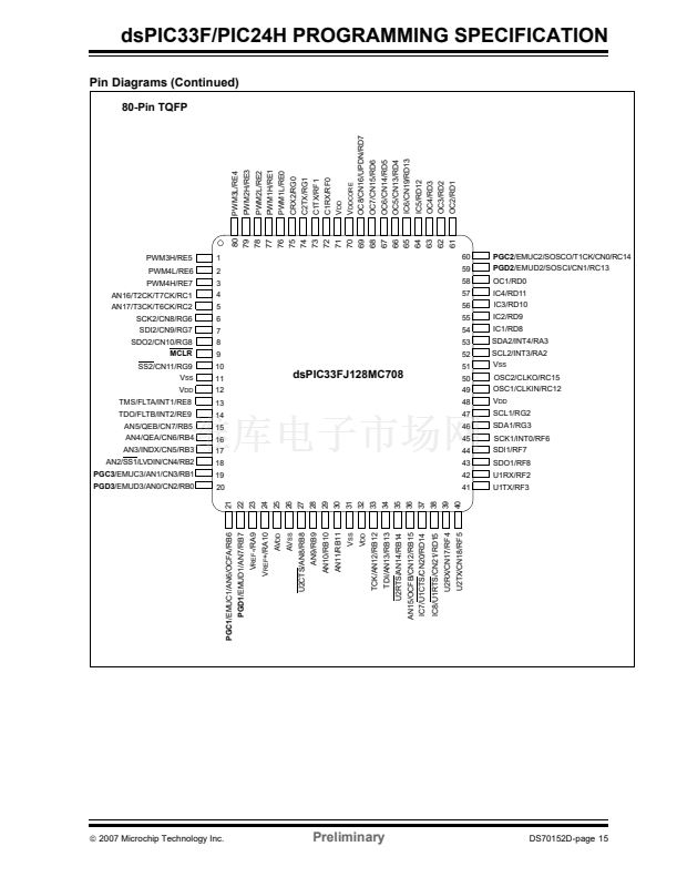
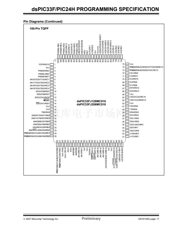
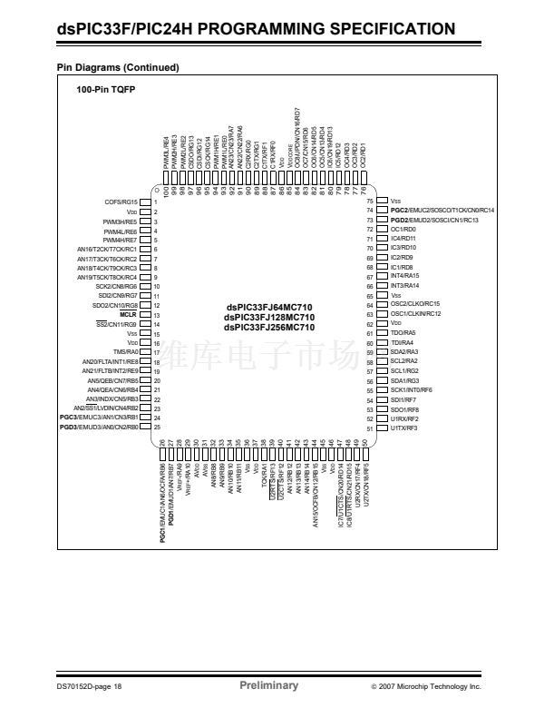
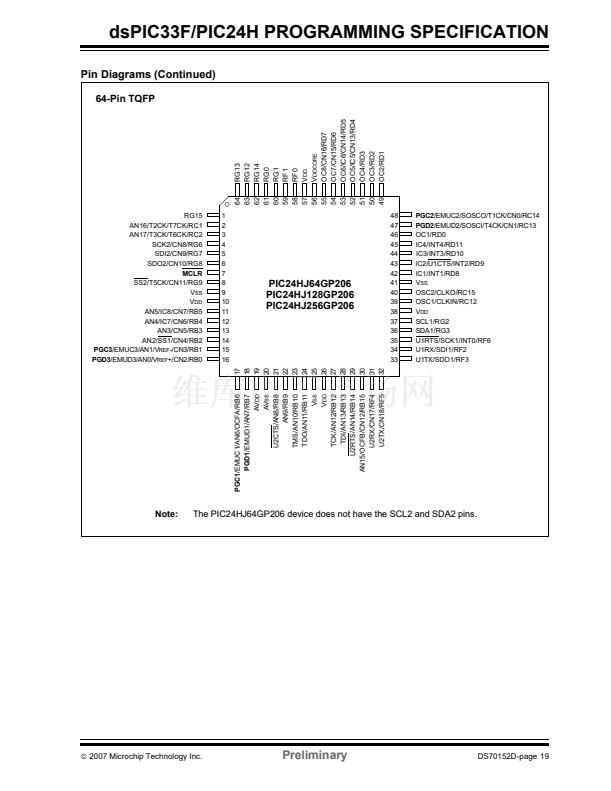
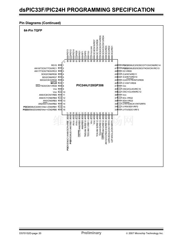
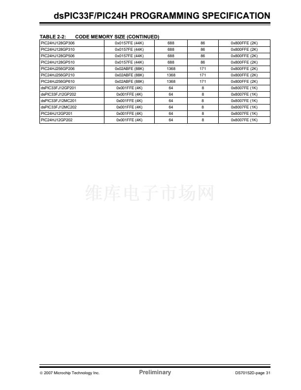
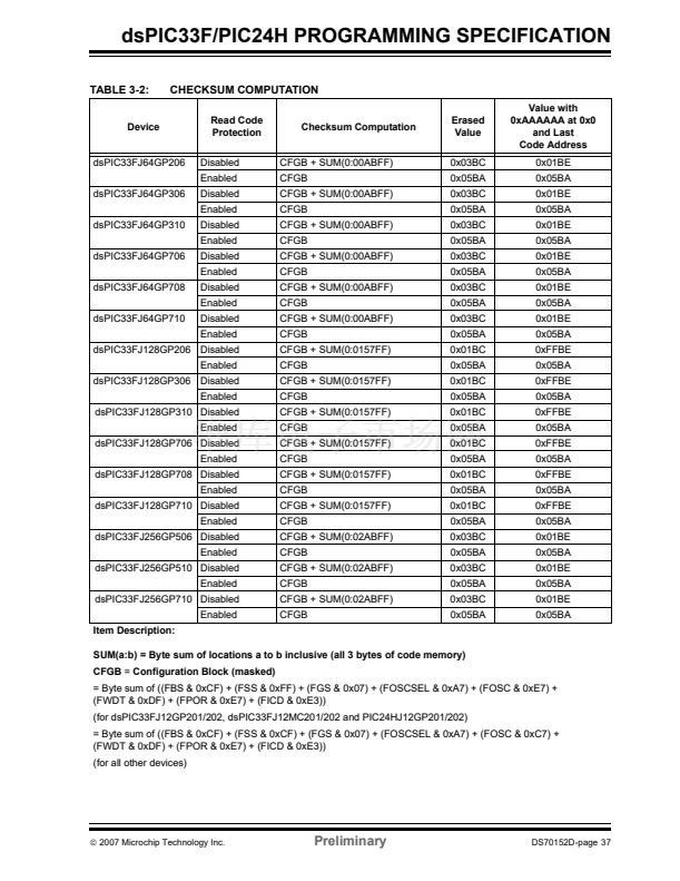
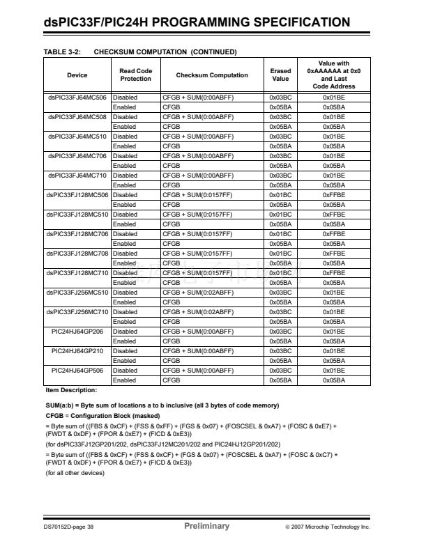
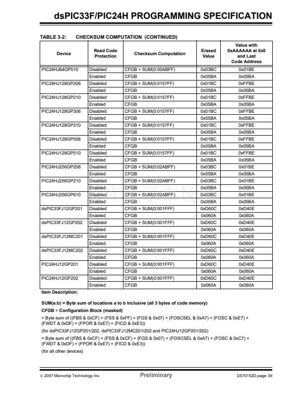
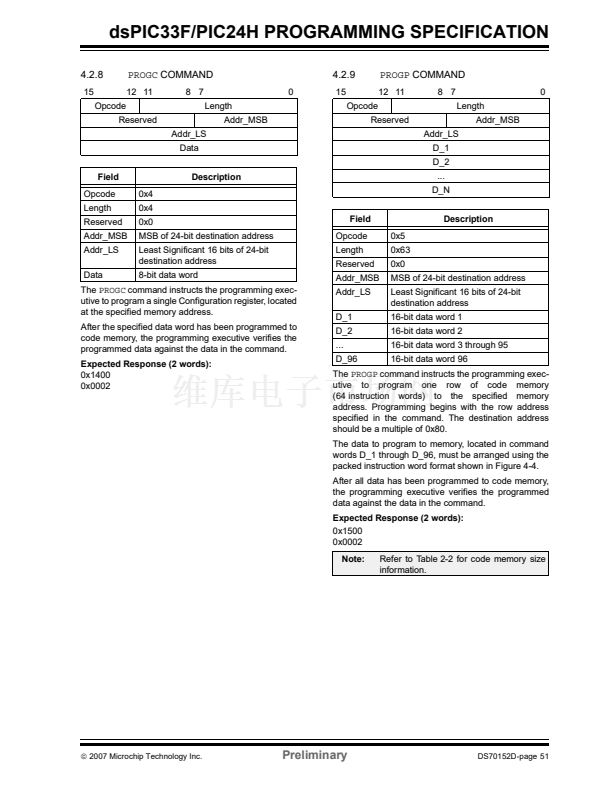
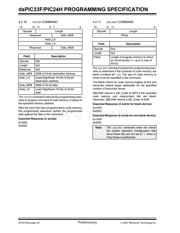
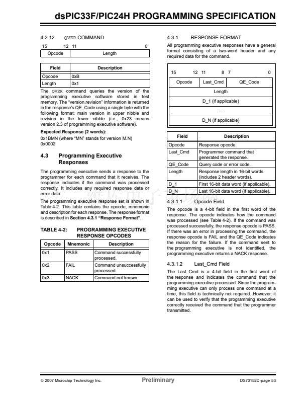
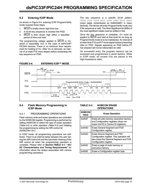
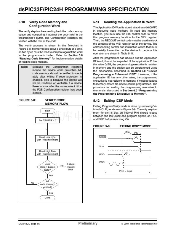
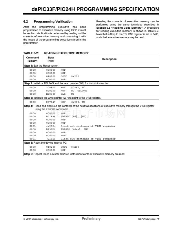
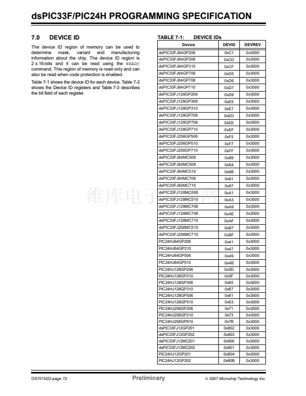
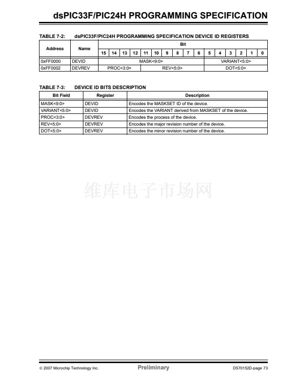
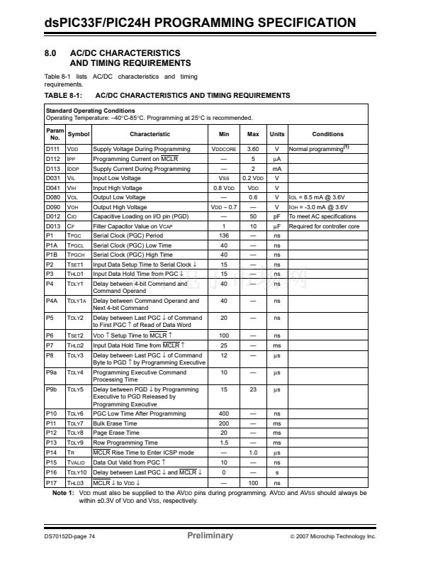
dsPIC33F/PIC24H PROGRAMMING SPECIFICATION
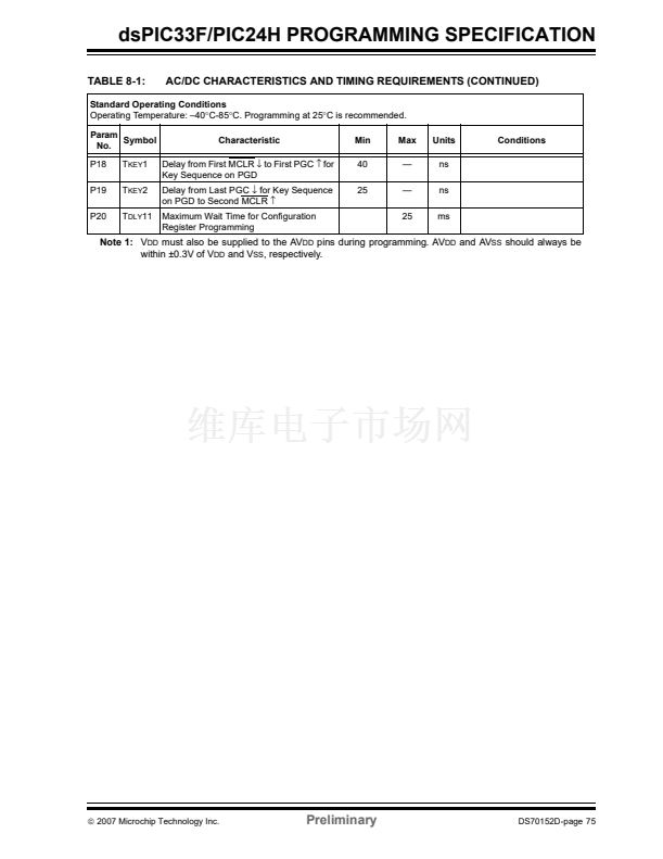
TABLE 3-3:
dsPIC33F/PIC24H CONFIGURATION BITS DESCRIPTION (CONTINUED)
Register
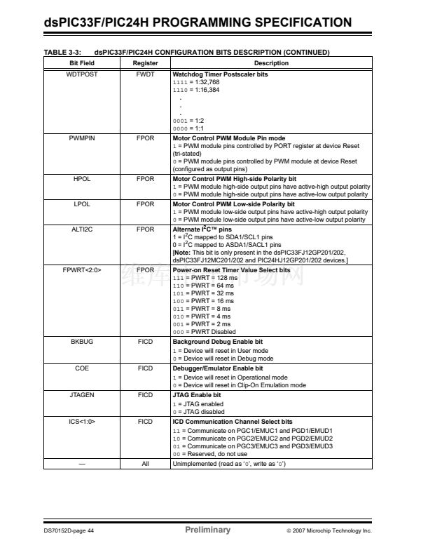
FWDT
Description
Watchdog Timer Postscaler bits
1111
= 1:32,768
1110
= 1:16,384
.
.
.
0001
= 1:2
0000
= 1:1
Motor Control PWM Module Pin mode
1
= PWM module pins controlled by PORT register at device Reset
(tri-stated)
0
= PWM module pins controlled by PWM module at device Reset
(configured as output pins)
Motor Control PWM High-side Polarity bit
1
= PWM module high-side output pins have active-high output polarity
0
= PWM module high-side output pins have active-low output polarity
Motor Control PWM Low-side Polarity bit
1
= PWM module low-side output pins have active-high output polarity
0
= PWM module low-side output pins have active-low output polarity
Alternate I
2
C鈩?pins
1 = I
2
C mapped to SDA1/SCL1 pins
0 = I
2
C mapped to ASDA1/SACL1 pins
[Note: This bit is only present in the dsPIC33FJ12GP201/202,
dsPIC33FJ12MC201/202 and PIC24HJ12GP201/202 devices.]
Power-on Reset Timer Value Select bits
111
= PWRT = 128 ms
110
= PWRT = 64 ms
101
= PWRT = 32 ms
100
= PWRT = 16 ms
011
= PWRT = 8 ms
010
= PWRT = 4 ms
001
= PWRT = 2 ms
000
= PWRT Disabled
Background Debug Enable bit
1
= Device will reset in User mode
0
= Device will reset in Debug mode
Debugger/Emulator Enable bit
1
= Device will reset in Operational mode
0
= Device will reset in Clip-On Emulation mode
JTAG Enable bit
1
= JTAG enabled
0
= JTAG disabled
ICD Communication Channel Select bits
11
= Communicate on PGC1/EMUC1 and PGD1/EMUD1
10
= Communicate on PGC2/EMUC2 and PGD2/EMUD2
01
= Communicate on PGC3/EMUC3 and PGD3/EMUD3
00
= Reserved, do not use
Unimplemented (read as 鈥?鈥? write as 鈥?鈥?
Bit Field
WDTPOST
PWMPIN
FPOR
HPOL
FPOR
LPOL
FPOR
ALTI2C
FPOR
FPWRT<2:0>
FPOR
BKBUG
FICD
COE
FICD
JTAGEN
FICD
ICS<1:0>
FICD
鈥?/div>
All
DS70152D-page 44
Preliminary
漏
2007 Microchip Technology Inc.


 1
1
 2
2
 3
3
 4
4
 5
5
 6
6
 7
7
 8
8
 9
9
 10
10
 11
11
 12
12
 13
13
 14
14
 15
15
 16
16
 17
17
 18
18
 19
19
 20
20
 21
21
 22
22
 23
23
 24
24
 25
25
 26
26
 27
27
 28
28
 29
29
 30
30
 31
31
 32
32
 33
33
 34
34
 35
35
 36
36
 37
37
 38
38
 39
39
 40
40
 41
41
 42
42
 43
43
 44
44
 45
45
 46
46
 47
47
 48
48
 49
49
 50
50
 51
51
 52
52
 53
53
 54
54
 55
55
 56
56
 57
57
 58
58
 59
59
 60
60
 61
61
 62
62
 63
63
 64
64
 65
65
 66
66
 67
67
 68
68
 69
69
 70
70
 71
71
 72
72
 73
73
 74
74
 75
75
 76
76
 77
77
 78
78
 79
79
 80
80
