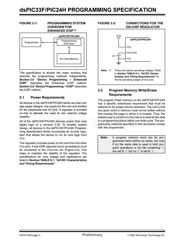
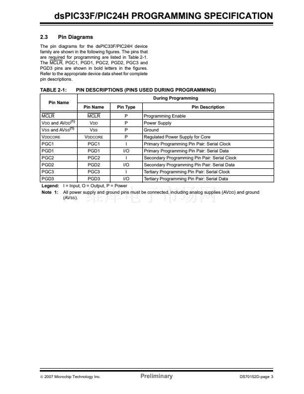
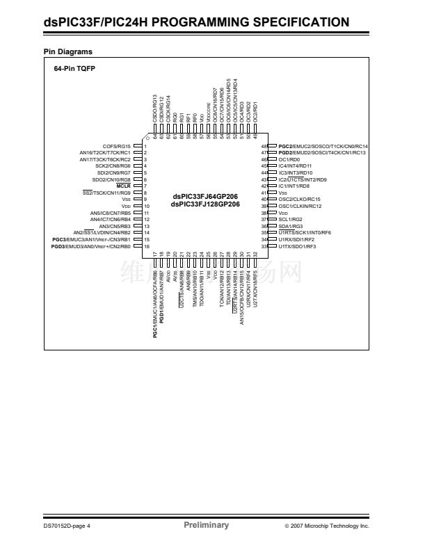
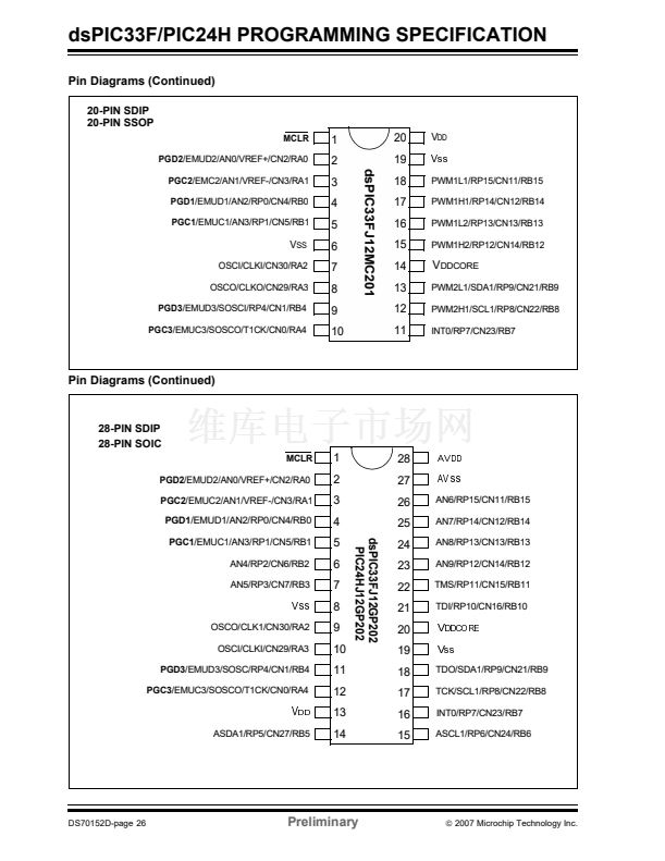
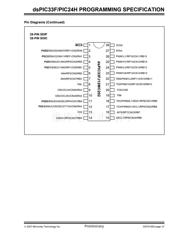
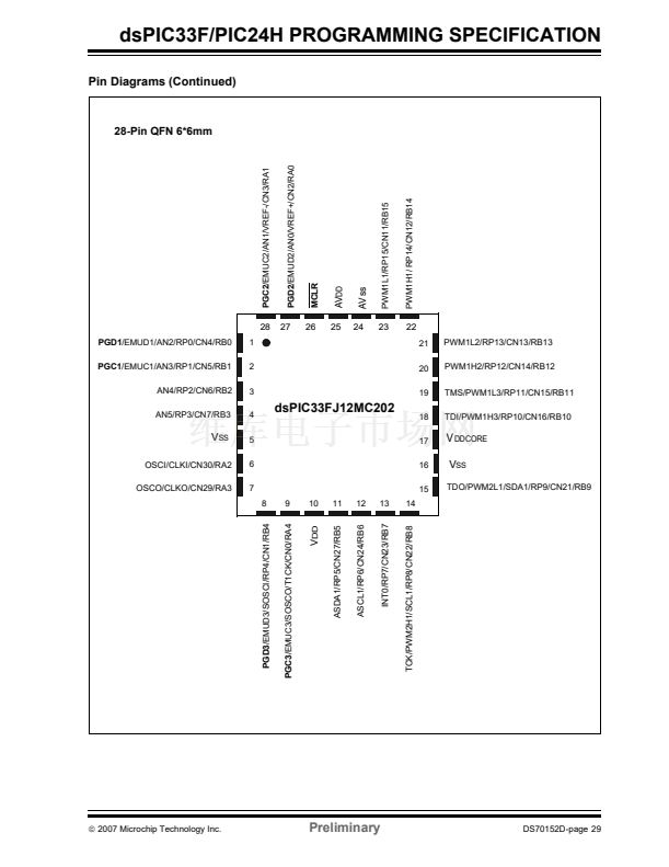
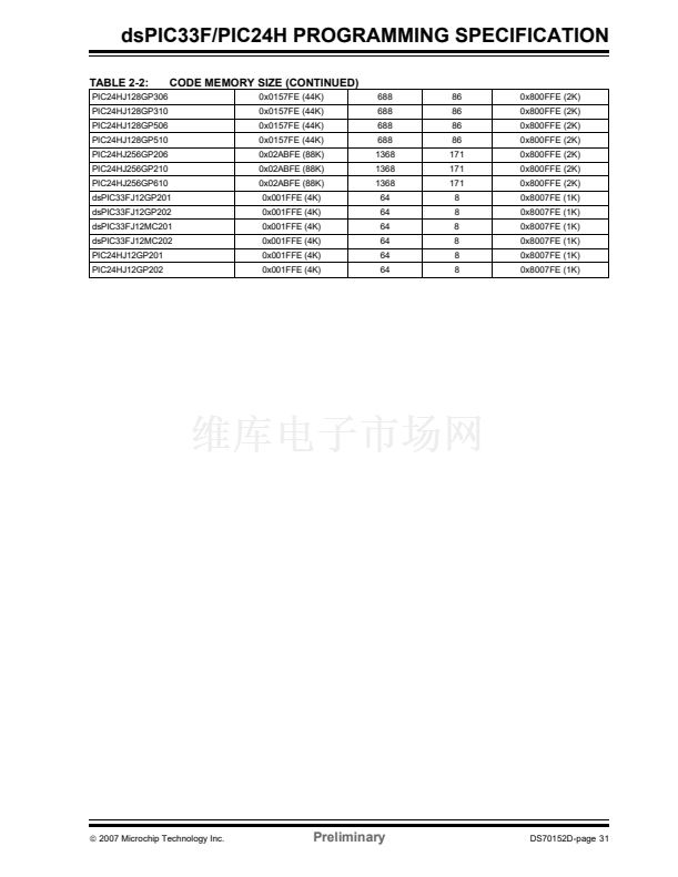
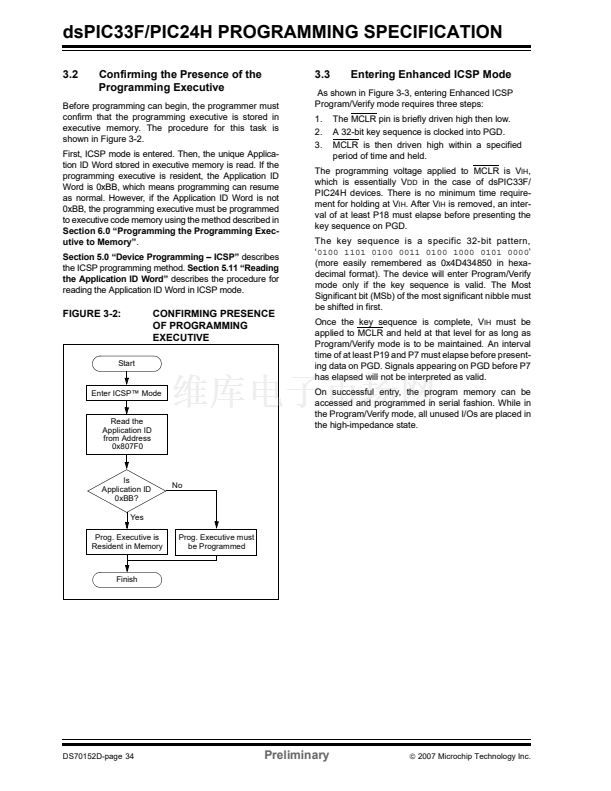
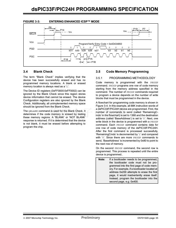
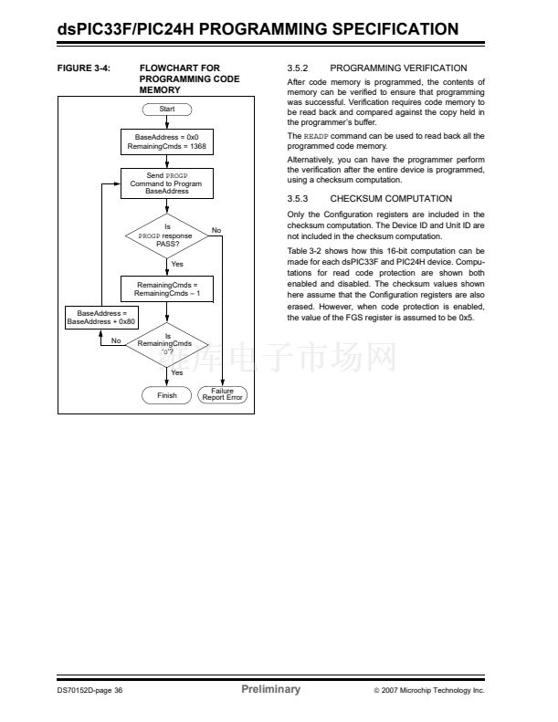
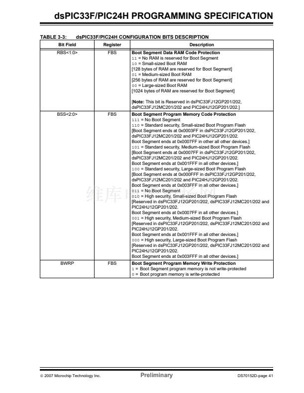
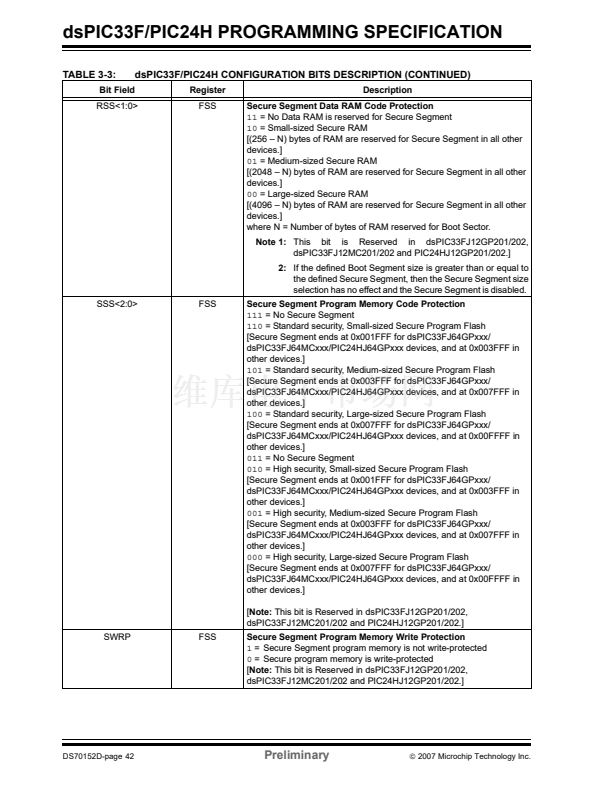
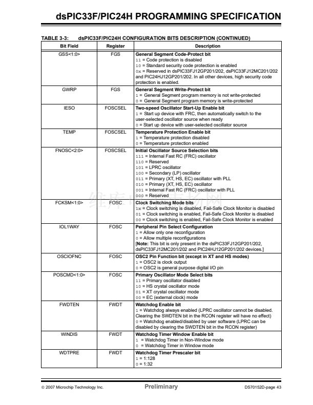
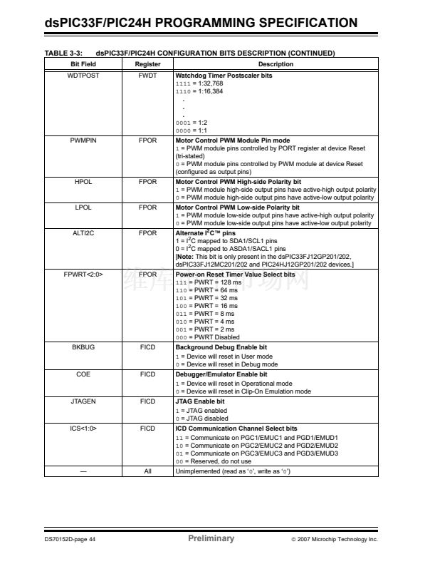
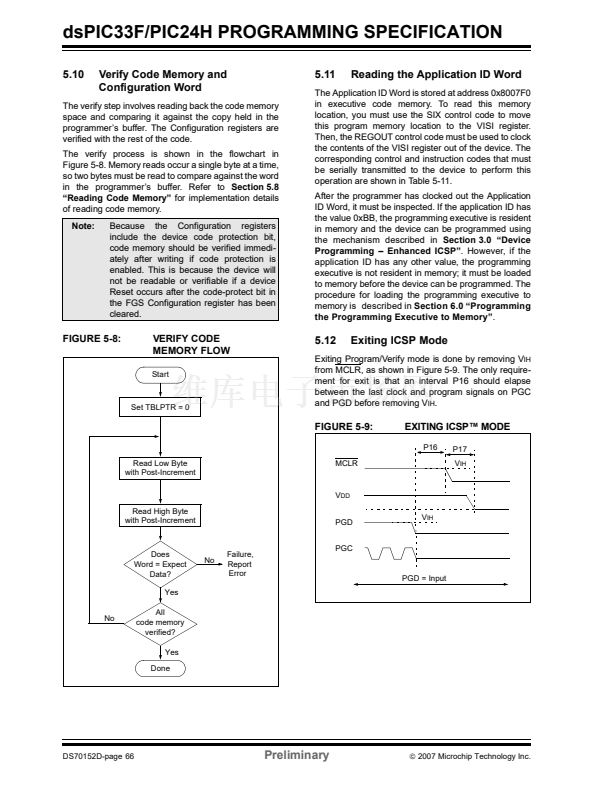
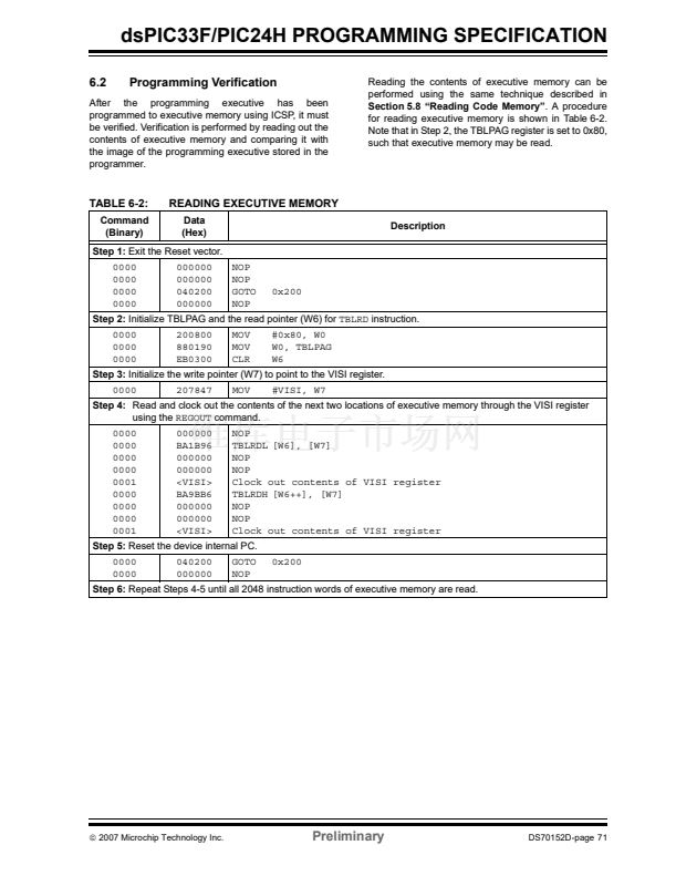
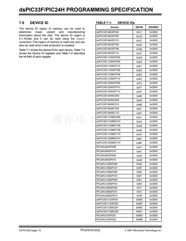
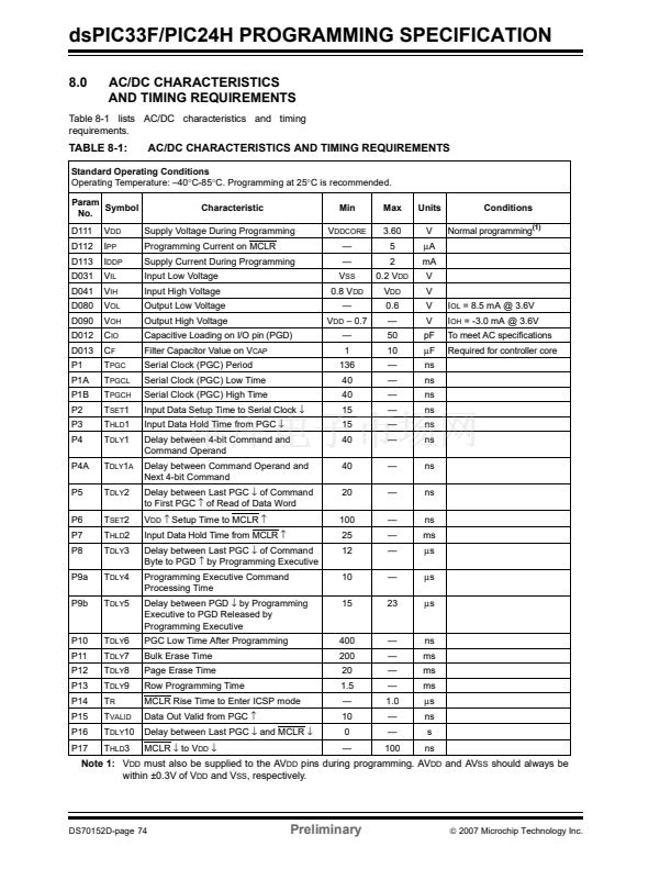
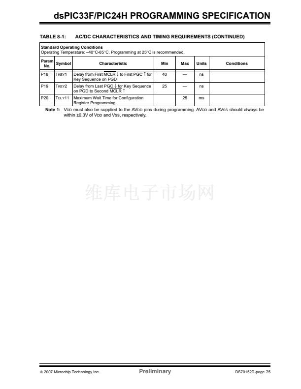
dsPIC33F/PIC24H PROGRAMMING SPECIFICATION
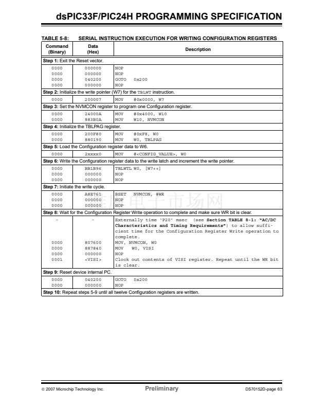
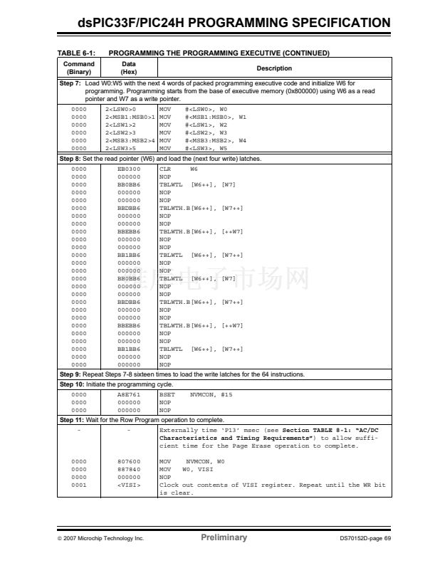
TABLE 5-8:
Command
(Binary)
SERIAL INSTRUCTION EXECUTION FOR WRITING CONFIGURATION REGISTERS
Data
(Hex)
Description
Step 1:
Exit the Reset vector.
0000
0000
0000
0000
0000
0000
0000
0000
0000
0000
0000
0000
0000
0000
0000
0000
-
000000
000000
040200
000000
200007
24000A
883B0A
200F80
880190
2xxxx0
BB1B96
000000
000000
A8E761
000000
000000
-
NOP
NOP
GOTO
NOP
MOV
MOV
MOV
MOV
MOV
MOV
0x200
Step 2:
Initialize the write pointer (W7) for the
TBLWT
instruction.
#0x0000, W7
#0x4000, W10
W10, NVMCON
#0xF8, W0
W0, TBLPAG
#<CONFIG_VALUE>, W0
Step 3:
Set the NVMCON register to program one Configuration register.
Step 4:
Initialize the TBLPAG register.
Step 5:
Load the Configuration register data to W6.
Step 6:
Write the Configuration register data to the write latch and increment the write pointer.
TBLWTL W0, [W7++]
NOP
NOP
BSET
NOP
NOP
NVMCON, #WR
Step 7:
Initiate the write cycle.
Step 8:
Wait for the Configuration Register Write operation to complete and make sure WR bit is clear.
Externally time 鈥楶20鈥?msec (see
Section TABLE 8-1: 鈥淎C/DC
Characteristics and Timing Requirements鈥?
to allow suffi-
cient time for the Configuration Register Write operation to
complete.
MOV, NVMCON, W0
MOV
W0, VISI
NOP
Clock out contents of VISI register. Repeat until the WR bit
is clear.
GOTO
NOP
0x200
0000
0000
0000
0001
807600
887840
000000
<VISI>
Step 9:
Reset device internal PC.
0000
0000
040200
000000
Step 10:
Repeat steps 5-9 until all twelve Configuration registers are written.
漏
2007 Microchip Technology Inc.
Preliminary
DS70152D-page 63


 1
1
 2
2
 3
3
 4
4
 5
5
 6
6
 7
7
 8
8
 9
9
 10
10
 11
11
 12
12
 13
13
 14
14
 15
15
 16
16
 17
17
 18
18
 19
19
 20
20
 21
21
 22
22
 23
23
 24
24
 25
25
 26
26
 27
27
 28
28
 29
29
 30
30
 31
31
 32
32
 33
33
 34
34
 35
35
 36
36
 37
37
 38
38
 39
39
 40
40
 41
41
 42
42
 43
43
 44
44
 45
45
 46
46
 47
47
 48
48
 49
49
 50
50
 51
51
 52
52
 53
53
 54
54
 55
55
 56
56
 57
57
 58
58
 59
59
 60
60
 61
61
 62
62
 63
63
 64
64
 65
65
 66
66
 67
67
 68
68
 69
69
 70
70
 71
71
 72
72
 73
73
 74
74
 75
75
 76
76
 77
77
 78
78
 79
79
 80
80
