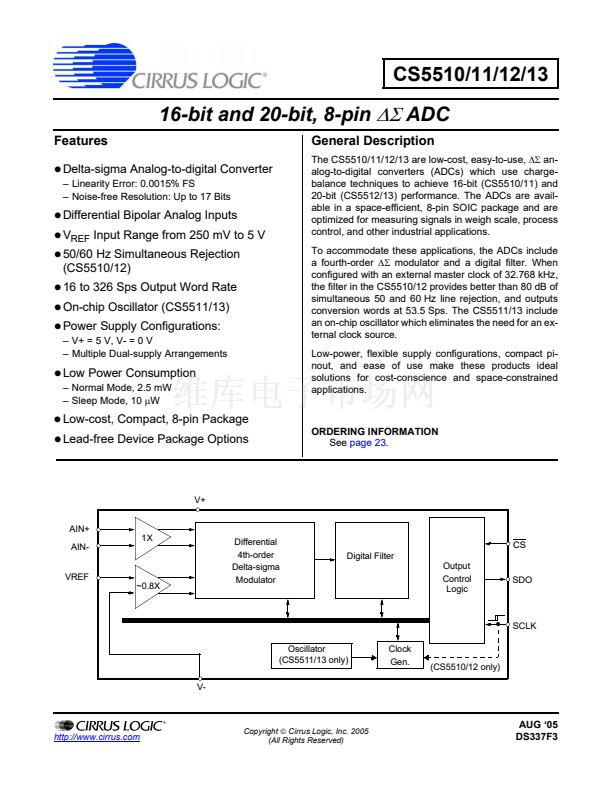
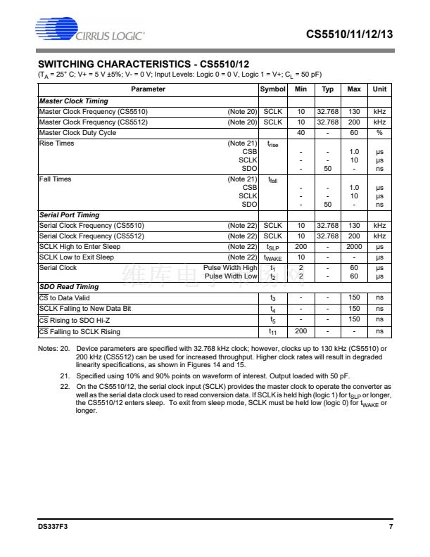
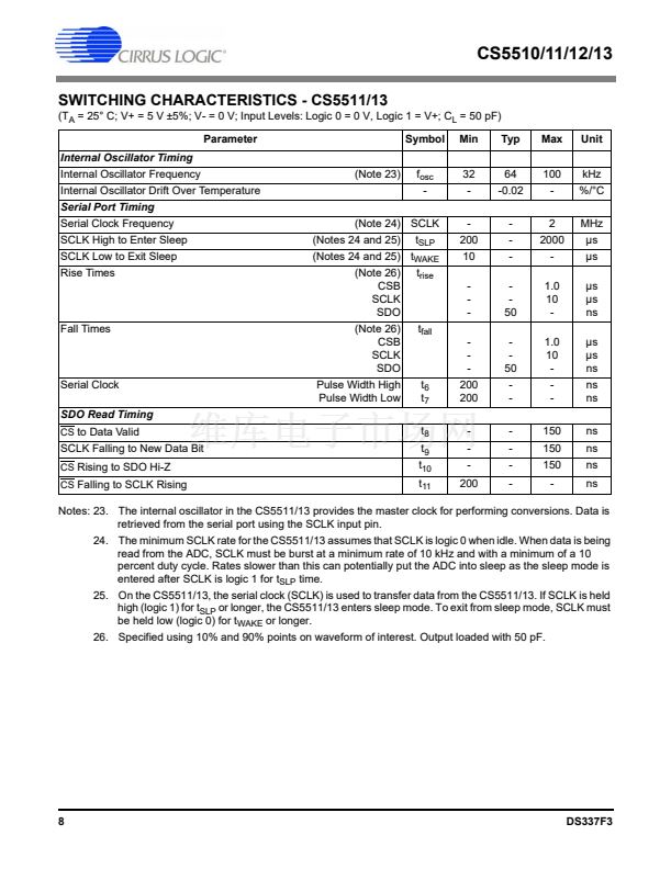
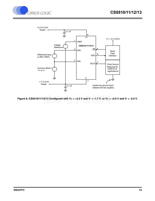
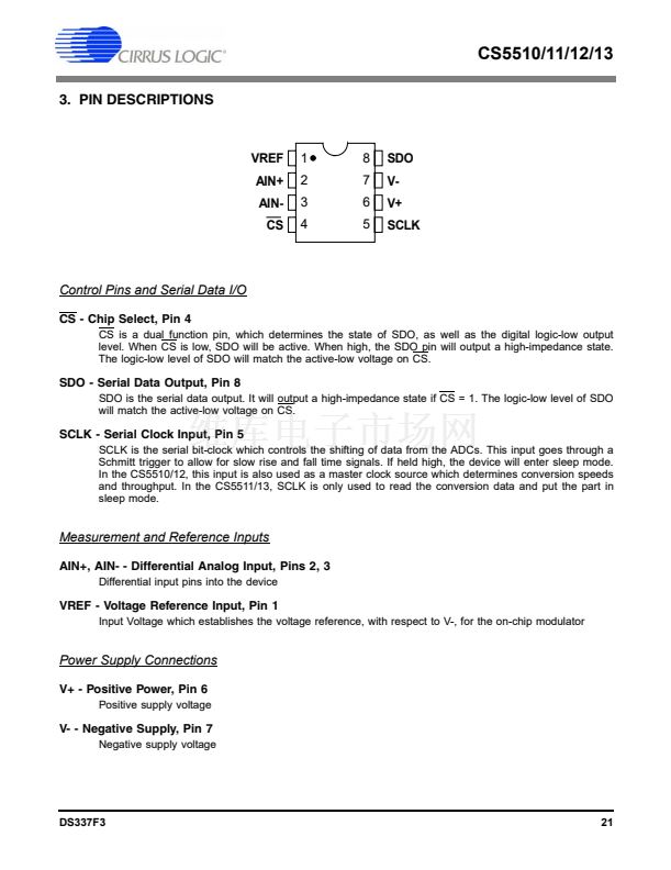
CS5510/11/12/13
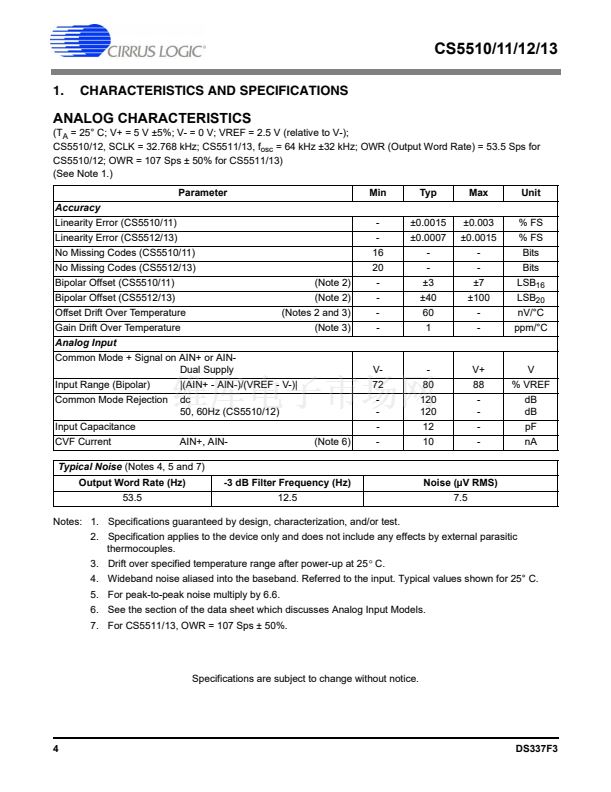
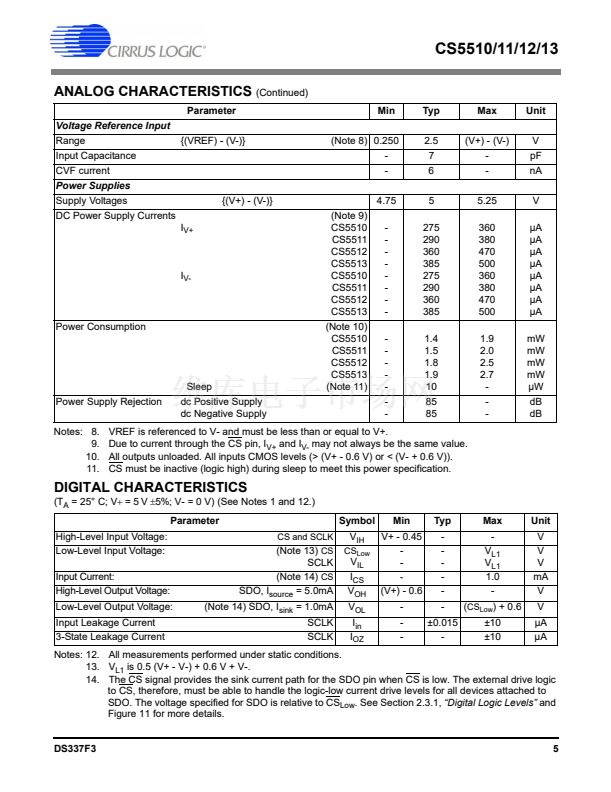
ANALOG CHARACTERISTICS
(Continued)
Parameter
Voltage Reference Input
Range
Input Capacitance
CVF current
Power Supplies
Supply Voltages
DC Power Supply Currents
I
V+
{(V+) - (V-)}
(Note 9)
CS5510
CS5511
CS5512
CS5513
CS5510
CS5511
CS5512
CS5513
(Note 10)
CS5510
CS5511
CS5512
CS5513
(Note 11)
4.75
-
-
-
-
-
-
-
-
-
-
-
-
-
-
-
5
275
290
360
385
275
290
360
385
1.4
1.5
1.8
1.9
10
85
85
5.25
360
380
470
500
360
380
470
500
1.9
2.0
2.5
2.7
-
-
-
V
碌A
碌A
碌A
碌A
碌A
碌A
碌A
碌A
mW
mW
mW
mW
碌W
dB
dB
{(VREF) - (V-)}
(Note 8) 0.250
-
-
2.5
7
6
(V+) - (V-)
-
-
V
pF
nA
Min
Typ
Max
Unit
I
V-
Power Consumption
Sleep
Power Supply Rejection
Notes: 8.
9.
10.
11.
dc Positive Supply
dc Negative Supply
VREF is referenced to V- and must be less than or equal to V+.
Due to current through the CS pin, I
V+
and I
V-
may not always be the same value.
All outputs unloaded. All inputs CMOS levels (> (V+ - 0.6 V) or < (V- + 0.6 V)).
CS must be inactive (logic high) during sleep to meet this power specification.
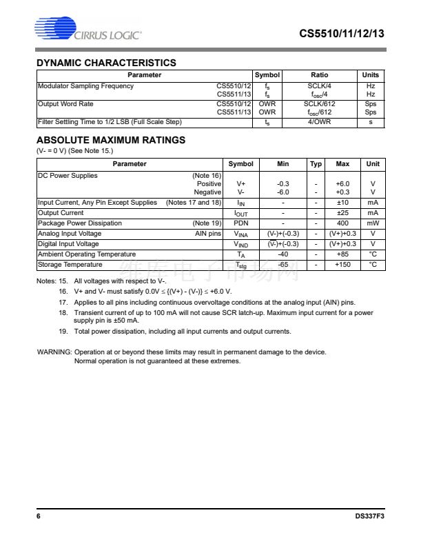
DIGITAL CHARACTERISTICS
(T
A
= 25擄 C; V+ = 5 V
鹵5%;
V- = 0 V) (See Notes 1 and 12.)
Parameter
High-Level Input Voltage:
Low-Level Input Voltage:
Input Current:
High-Level Output Voltage:
Low-Level Output Voltage:
Input Leakage Current
3-State Leakage Current
CS and SCLK
Symbol
V
IH
CS
Low
Min
V+ - 0.45
-
-
-
Typ
-
-
-
-
-
-
鹵0.015
-
Max
-
V
L1
V
L1
1.0
-
(
CS
Low
) + 0.6
鹵10
鹵10
Unit
V
V
V
mA
V
V
碌A
碌A
(Note 13)
CS
SCLK
(Note 14)
CS
SDO, I
source
= 5.0mA
(Note 14) SDO, I
sink
= 1.0mA
SCLK
SCLK
V
IL
I
CS
V
OH
V
OL
I
in
I
OZ
(V+) - 0.6
-
-
-
Notes: 12. All measurements performed under static conditions.
13. V
L1
is 0.5 (V+ - V-) + 0.6 V + V-.
14. The CS signal provides the sink current path for the SDO pin when CS is low. The external drive logic
to CS, therefore, must be able to handle the logic-low current drive levels for all devices attached to
SDO. The voltage specified for SDO is relative to CS
Low
. See Section 2.3.1,
鈥淒igital Logic Levels鈥?/span>
and
Figure 11 for more details.
DS337F3
5


 1
1
 2
2
 3
3
 4
4
 5
5
 6
6
 7
7
 8
8
 9
9
 10
10
 11
11
 12
12
 13
13
 14
14
 15
15
 16
16
 17
17
 18
18
 19
19
 20
20
 21
21
 22
22
 23
23
 24
24
