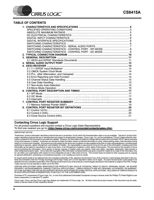
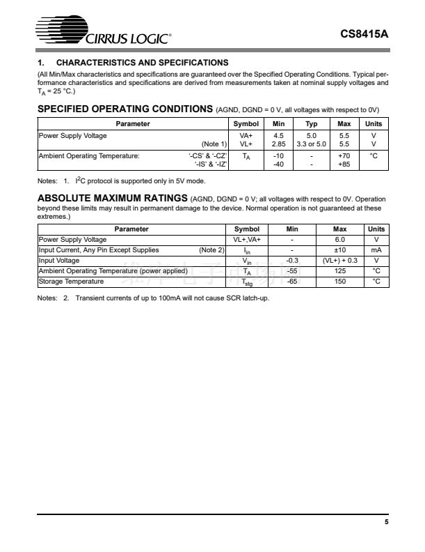
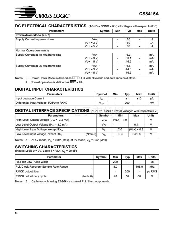
Default = 鈥?00鈥?/div>
000 - RXP0
001 - RXP1
010 - RXP2
011 - RXP3
100 - RXP4
101 - RXP5
110 - RXP6
111 - Reserved
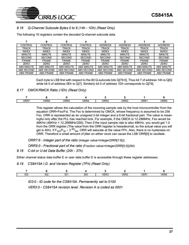
8.3
7
0
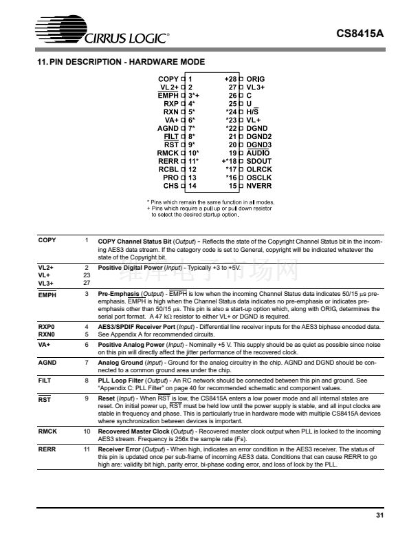
Clock Source Control (04h)
6
RUN
5
0
4
0
3
0
2
0
1
0
0
0
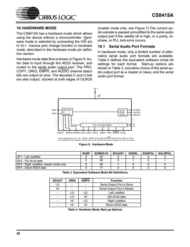
This register configures the clock sources of various blocks. In conjunction with the Data Flow Control register, var-
ious Receiver/Transmitter/Transceiver modes may be selected.
RUN - Controls the internal clocks, allowing the CS8415A to be placed in a 鈥減owered down鈥? low
current consumption, state.
Default = 鈥?鈥?/div>
0 - Internal clocks are stopped. Internal state machines are reset. The fully static control port is
operational, allowing registers to be read or changed. Reading and writing the U and C data
buffers is not possible. Power consumption is low.
1 - Normal part operation. This bit must be written to the 1 state to allow the CS8415A to begin
operation. All input clocks should be stable in frequency and phase when RUN is set to 1.
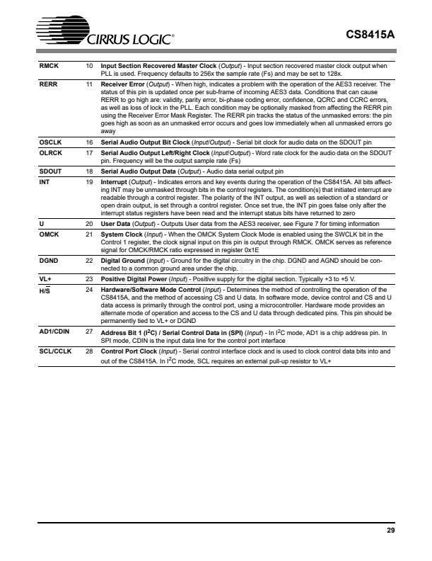
8.4
7
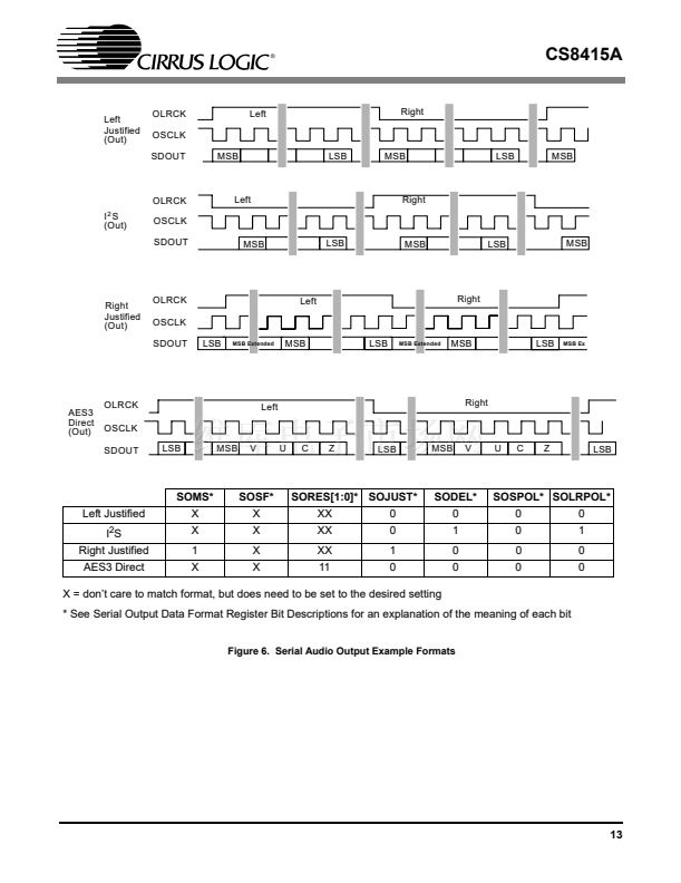
Serial Audio Output Port Data Format (06h)
6
SOSF
5
SORES1
4
SORES0
3
SOJUST
2
SODEL
1
SOSPOL
0
SOLRPOL
SOMS
SOMS - Master/Slave Mode Selector
Default = 鈥?鈥?/div>
0 - Serial audio output port is in slave mode
1 - Serial audio output port is in master mode
SOSF - OSCLK frequency (for master mode)
Default = 鈥?鈥?/div>
0 - 64*Fs
1 - 128*Fs
SORES1:0 - Resolution of the output data on SDOUT
Default = 鈥?0鈥?/div>
00 - 24-bit resolution
01 - 20-bit resolution
10 - 16-bit resolution
11 - Direct copy of the received NRZ data from the AES3 receiver (including C, U, and V bits,
the time slot normally occupied by the P bit is used to indicate the location of the block start,
21


 1
1
 2
2
 3
3
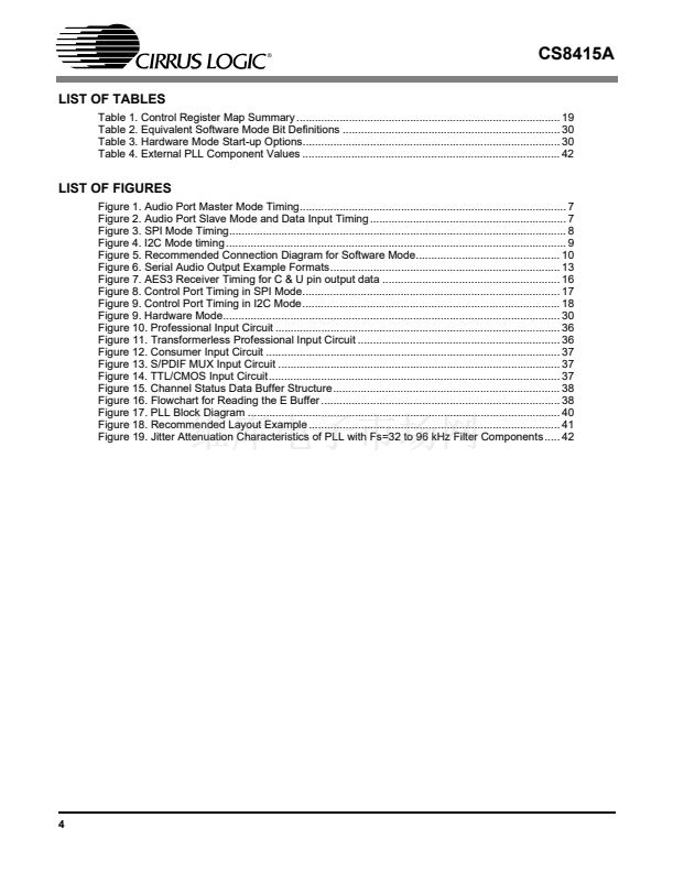 4
4
 5
5
 6
6
 7
7
 8
8
 9
9
 10
10
 11
11
 12
12
 13
13
 14
14
 15
15
 16
16
 17
17
 18
18
 19
19
 20
20
 21
21
 22
22
 23
23
 24
24
 25
25
 26
26
 27
27
 28
28
 29
29
 30
30
 31
31
 32
32
 33
33
 34
34
 35
35
 36
36
 37
37
 38
38
 39
39
 40
40
 41
41
 42
42
