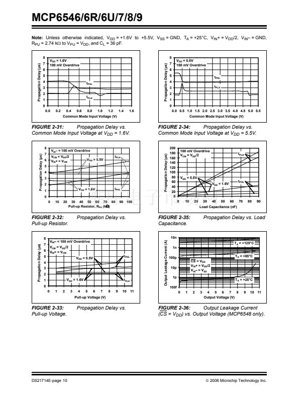
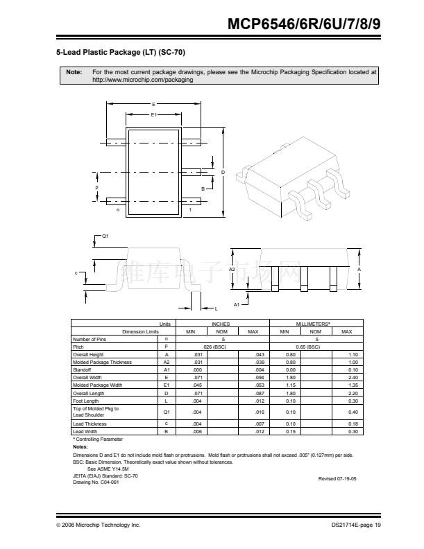
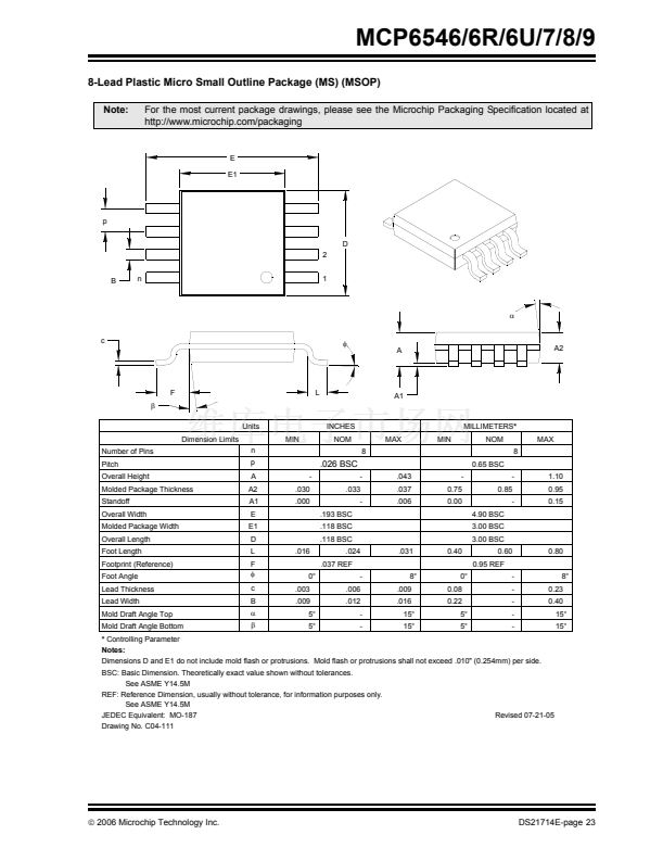
鈥?/div>
V
OUT
25
20
15
10
5
0
-5
-10
-15
-20
-25
-30
Input Voltage (10 mV/div)
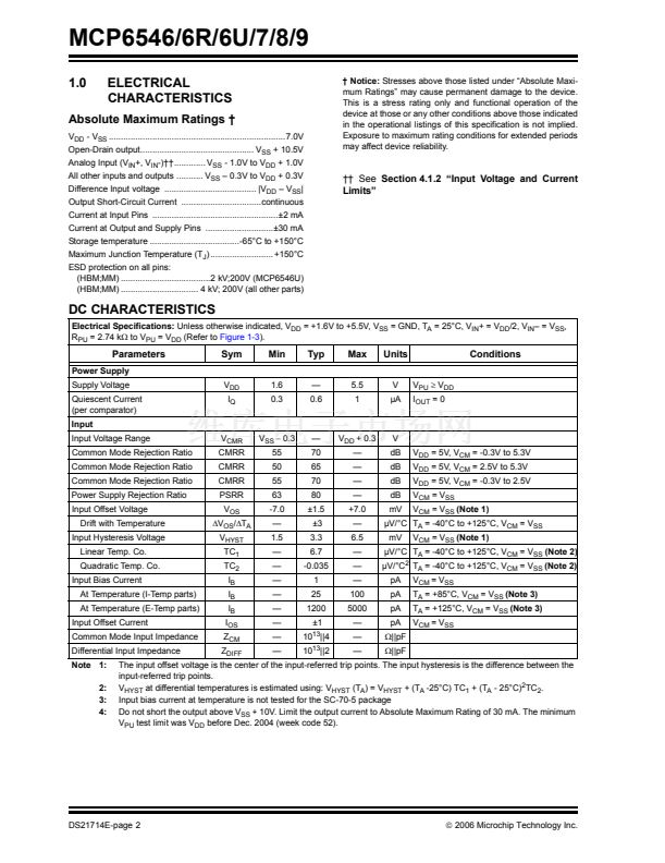
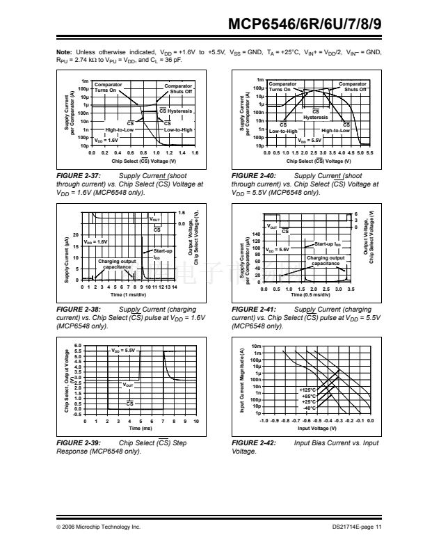
INVERTING CIRCUIT
Output Voltage (V)
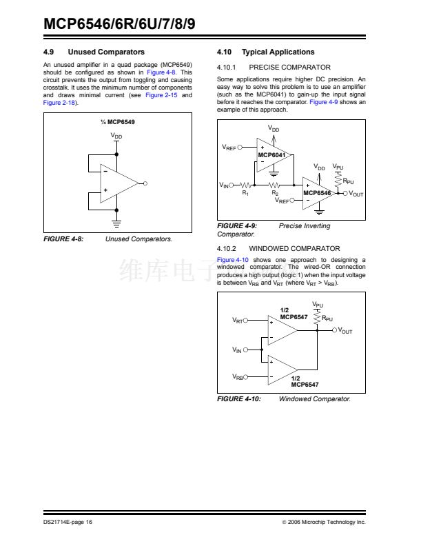
Figure 4-4
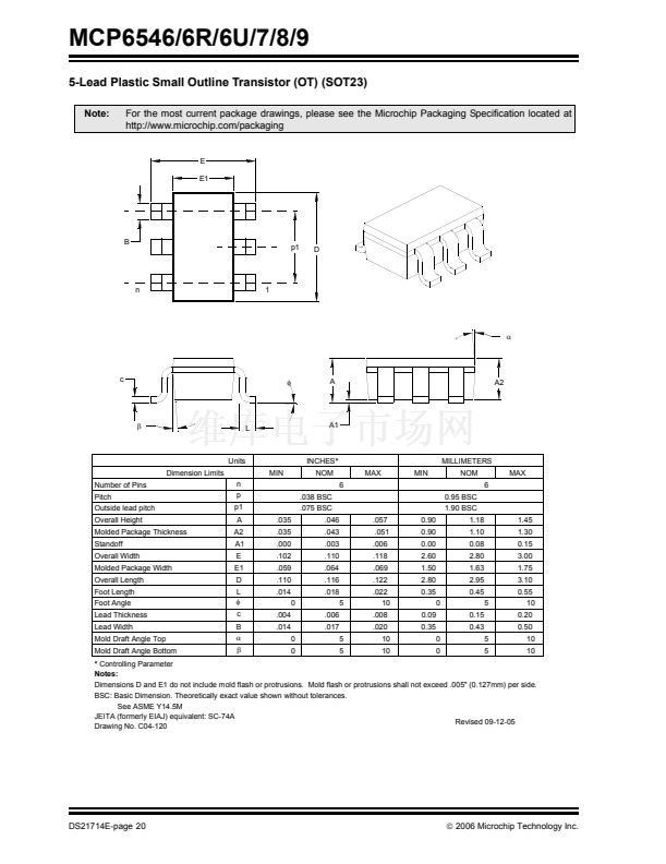
shows an inverting circuit for a single-supply
application using three resistors, besides the pull-up
resistor. The resulting hysteresis diagram is shown in
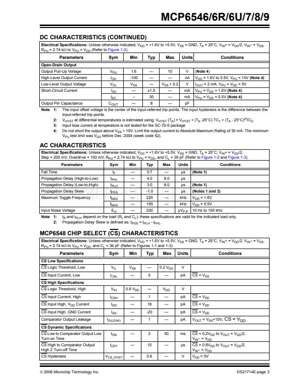
Figure 4-5.
V
DD
V
IN
V
DD
R
2
MCP654X
V
PU
Hysteresis
I
PU
I
OL
I
RF
R
F
R
PU
V
OUT
Time (100 ms/div)
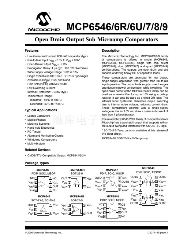
FIGURE 4-3:
The MCP6546/7/8/9
comparators鈥?internal hysteresis eliminates
output chatter caused by input noise voltage.
R
3
4.2
Open-Drain Output
FIGURE 4-4:
hysteresis.
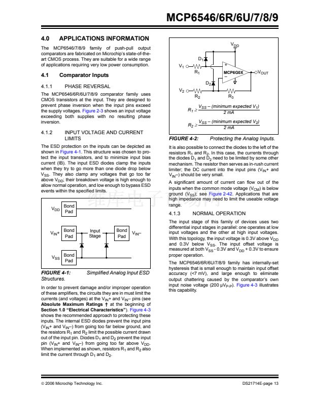
V
OUT
V
PU
V
OH
Low-to-High
V
OL
V
SS
V
SS
High-to-Low
V
IN
V
TLH
V
THL
V
DD
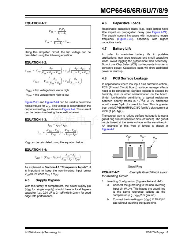
The open-drain output is designed to make level-
shifting and wired-OR logic easy to implement. The
output can go as high as 10V for 9V battery-powered
applications. The output stage minimizes switching cur-
rent (shoot-through current from supply-to-supply)
when the output changes state. See Figures 2-15, 2-18
and 2-37 through 2-41, for more information.
Inverting circuit with
4.3
MCP6548 Chip Select (CS)
The MCP6548 is a single comparator with a Chip
Select (CS) pin. When CS is pulled high, the total
current consumption drops to 20 pA (typ.). 1 pA (typ.)
flows through the CS pin, 1 pA (typ.) flows through the
output pin and 18 pA (typ.) flows through the V
DD
pin,
as shown in
Figure 1-1.
When this happens, the
comparator output is put into a high-impedance state.
By pulling CS low, the comparator is enabled. If the CS
pin is left floating, the comparator will not operate
properly.
Figure 1-1
shows the output voltage and
supply current response to a CS pulse.
The internal CS circuitry is designed to minimize
glitches when cycling the CS pin. This helps conserve
power, which is especially important in battery-powered
applications.
V
TLH
= trip voltage from low to high
V
THL
= trip voltage from high to low
FIGURE 4-5:
inverting circuit.
Hysteresis diagram for the
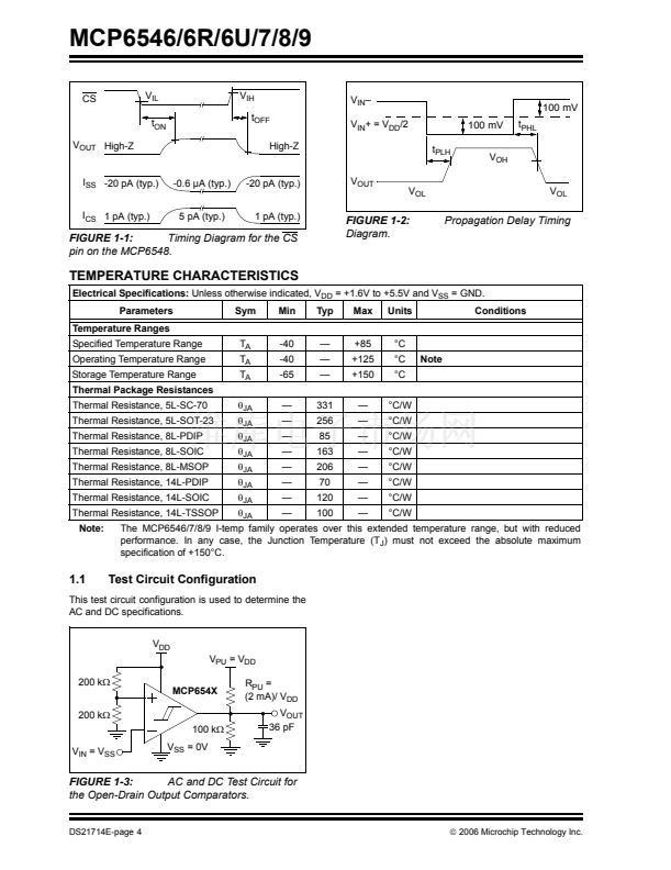
In order to determine the trip voltages (V
THL
and V
TLH
)
for the circuit shown in
Figure 4-4,
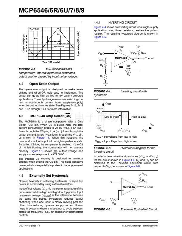
R
2
and R
3
can be
simplified to the Thevenin equivalent circuit with
respect to V
DD
, as shown in
Figure 4-6.
V
PU
-
MCP654X
+
V
23
R
23
R
F
R
PU
V
OUT
4.4
Externally Set Hysteresis
Greater flexibility in selecting hysteresis, or input trip
points, is achieved by using external resistors.
Input offset voltage (V
OS
) is the center (average) of the
(input-referred) low-high and high-low trip points. Input
hysteresis voltage (V
HYST
) is the difference between
the same trip points. Hysteresis reduces output
chattering when one input is slowly moving past the
other, thus reducing dynamic supply current. It also
helps in systems where it is best not to cycle between
states too frequently (e.g., air conditioner thermostatic
control).
FIGURE 4-6:
Thevenin Equivalent Circuit.
DS21714E-page 14
漏
2006 Microchip Technology Inc.


 1
1
 2
2
 3
3
 4
4
 5
5
 6
6
 7
7
 8
8
 9
9
 10
10
 11
11
 12
12
 13
13
 14
14
 15
15
 16
16
 17
17
 18
18
 19
19
 20
20
 21
21
 22
22
 23
23
 24
24
 25
25
 26
26
 27
27
 28
28
 29
29
 30
30
 31
31
 32
32
