鈳?/div>
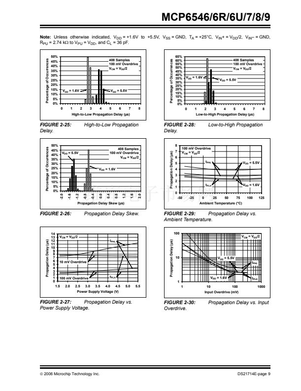
V
TLH
= trip voltage from low to high
V
THL
= trip voltage from high to low
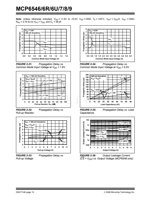
Figure 2-21
and
Figure 2-24
can be used to determine
typical values for V
OL
. This voltage is dependent on the
output current I
OL
as shown in
Figure 4-4.
This current
can be determined using the equation below:
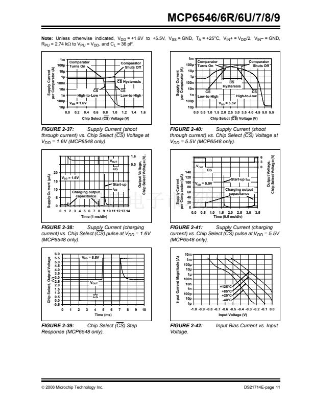
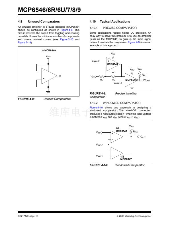
In order to maximize battery life in portable
applications, use large resistors and small capacitive
loads. Avoid toggling the output more than necessary.
Do not use Chip Select (CS) too frequently in order to
conserve power. Capacitive loads will draw additional
power at start-up.
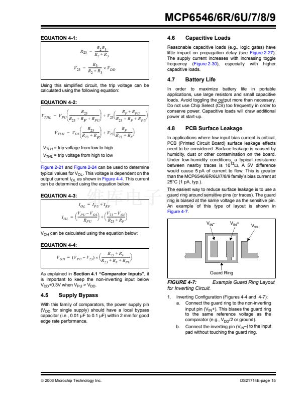
4.8
PCB Surface Leakage
In applications where low input bias current is critical,
PCB (Printed Circuit Board) surface leakage effects
need to be considered. Surface leakage is caused by
humidity, dust or other contamination on the board.
Under low-humidity conditions, a typical resistance
between nearby traces is 10
12
惟.
A 5V difference
would cause 5 pA of current to flow. This is greater
than the MCP6546/6R/6U/7/8/9 family鈥檚 bias current at
25擄C (1 pA, typ.).
The easiest way to reduce surface leakage is to use a
guard ring around sensitive pins (or traces). The guard
ring is biased at the same voltage as the sensitive pin.
An example of this type of layout is shown in
Figure 4-7.
V
IN
-
V
IN
+
V
SS
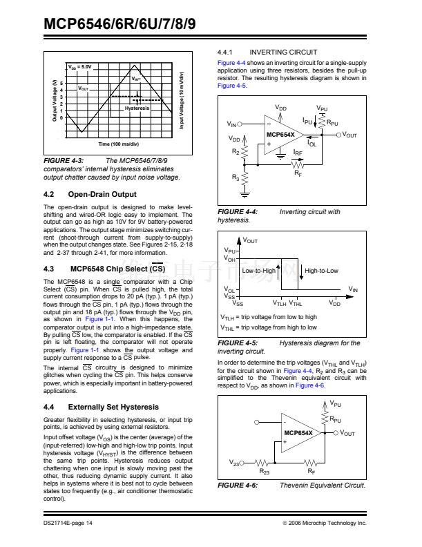
EQUATION 4-3:
I
OL
=
I
PU
+
I
RF
V
23
鈥?/div>
V
OL
V
PU
鈥?/div>
V
OL
-
I
OL
=
鈳?/div>
-------------------------
鈳?/div>
+
鈳?/div>
------------------------
鈳?/div>
鈳?/div>
R
PU
鈳?鈳?/div>
R
23
+
R
F
鈳?/div>
V
OH
can be calculated using the equation below:
EQUATION 4-4:
R
23
+
R
F
-
V
OH
=
(
V
PU
鈥?/div>
V
23
) 脳 鈳?/div>
-------------------------------------
鈳?/div>
鈳?/div>
R
23
+
R
F
+
R
PU
鈳?/div>
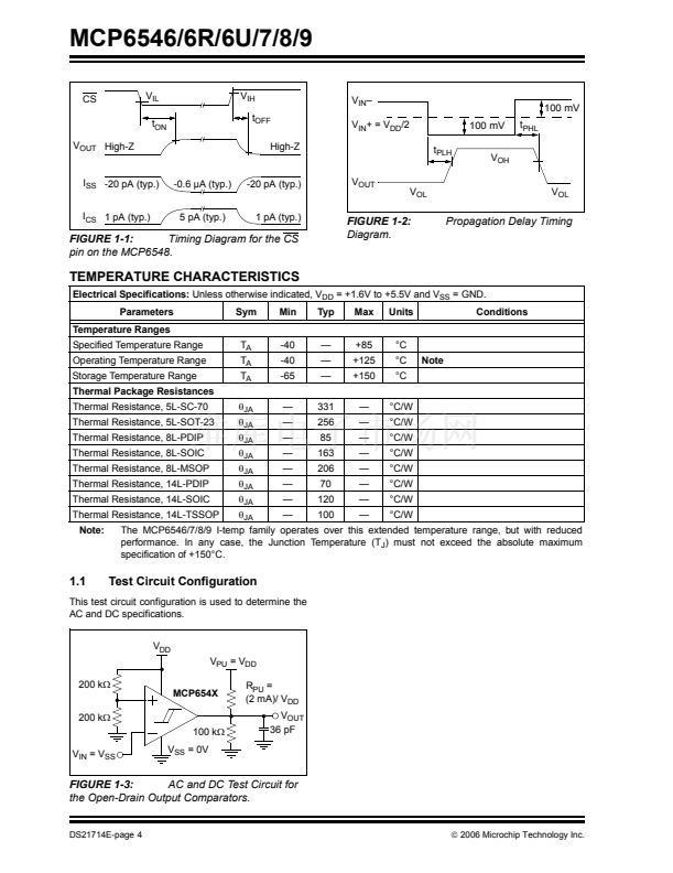
As explained in
Section 4.1 鈥淐omparator Inputs鈥?
it
is important to keep the non-inverting input below
V
DD
+0.3V when V
PU
> V
DD
.
Guard Ring
FIGURE 4-7:
Example Guard Ring Layout
for Inverting Circuit.
1.
Inverting Configuration (Figures 4-4 and 4-7):
a. Connect the guard ring to the non-inverting
input pin (V
IN
+). This biases the guard ring
to the same reference voltage as the
comparator (e.g., V
DD
/2 or ground).
b. Connect the inverting pin (V
IN
鈥? to the input
pad without touching the guard ring.
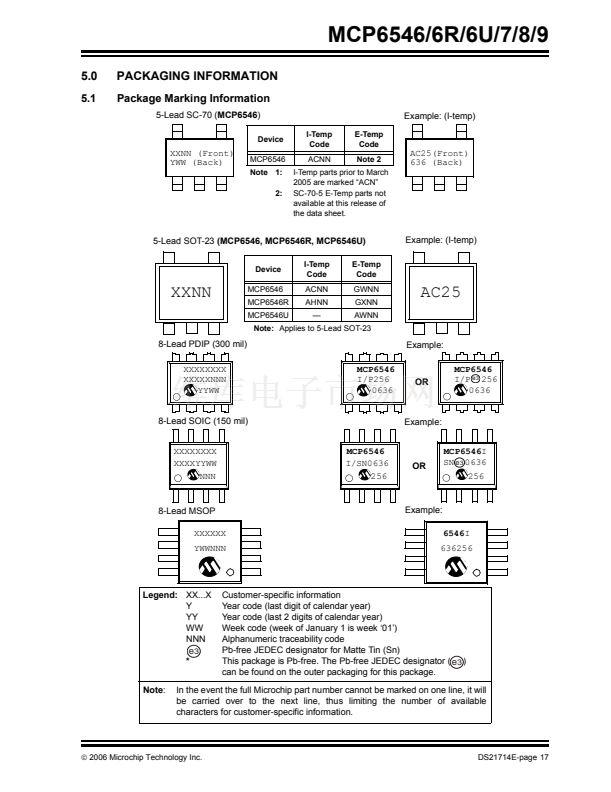
4.5
Supply Bypass
With this family of comparators, the power supply pin
(V
DD
for single supply) should have a local bypass
capacitor (i.e., 0.01 碌F to 0.1 碌F) within 2 mm for good
edge rate performance.
漏
2006 Microchip Technology Inc.
DS21714E-page 15
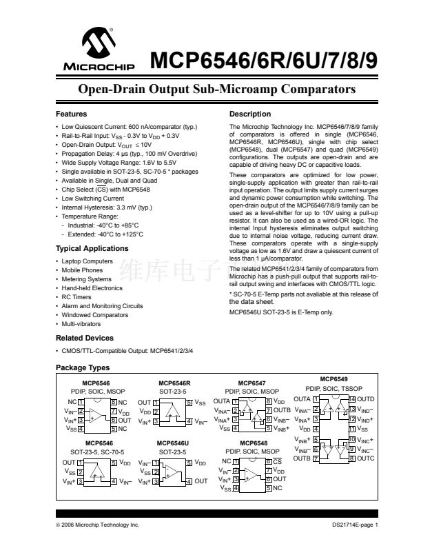
MCP6546T-I/LT 產(chǎn)品屬性
Microchip
校驗(yàn)器 IC
1 Channel
Analog Comparators
Open Drain
4 us
7 mV
1 uA
+ 85 C
SMD/SMT
SC-70-5
Reel
- 40 C
3000
5.5 V
1.6 V
MCP6546T-I/LT相關(guān)型號(hào)PDF文件下載
-
型號(hào)
版本
描述
廠商
下載
-
英文版
2.7V to 6.0V Single Supply CMOS Op Amps
-
英文版
2.7V to 5.5V Single Supply CMOS Op Amps
-
英文版
2.7V to 6.0V Single Supply CMOS Op Amps
-
英文版
2.7V to 5.5V Single Supply CMOS Op Amps
-
英文版
2.7V to 6.0V Single Supply CMOS Op Amps
-
英文版
2.7V to 5.5V Single Supply CMOS Op Amps
-
英文版
2.7V to 6.0V Single Supply CMOS Op Amps
-
英文版
2.7V to 5.5V Single Supply CMOS Op Amps
-
英文版
2.5V to 5.5V Micropower CMOS Op Amps
-
英文版
2.5V to 5.5V Micropower CMOS Op Amps
-
英文版
2.5V to 6.0V Micropower CMOS Op Amp
-
英文版
2.5V to 5.5V Micropower CMOS Op Amps
-
英文版
2.5V to 6.0V Micropower CMOS Op Amp
-
英文版
2.5V to 5.5V Micropower CMOS Op Amps
-
英文版
2.3V to 5.5V Micropower Bi-CMOS Op Amps
-
英文版
2.3V to 5.5V Micropower Bi-CMOS Op Amps
-
英文版
2.3V to 5.5V Micropower Bi-CMOS Op Amps
-
英文版
2.3V to 5.5V Micropower Bi-CMOS Op Amps
-
英文版
2.3V to 5.5V Micropower Bi-CMOS Op Amps
-
英文版
2.3V to 5.5V Micropower Bi-CMOS Op Amps


 1
1
 2
2
 3
3
 4
4
 5
5
 6
6
 7
7
 8
8
 9
9
 10
10
 11
11
 12
12
 13
13
 14
14
 15
15
 16
16
 17
17
 18
18
 19
19
 20
20
 21
21
 22
22
 23
23
 24
24
 25
25
 26
26
 27
27
 28
28
 29
29
 30
30
 31
31
 32
32
