鈥?/div>
Units
V
nA
V
mA
mA
pF
(Note
4)
Conditions
V
DD
= 1.6V to 5.5V, V
PU
= 10V
(Note 4)
I
OUT
= 2 mA, V
PU
= V
DD
= 5V
V
PU
= V
DD
= 1.6V
(Note 4)
V
PU
= V
DD
= 5.5V
(Note 4)
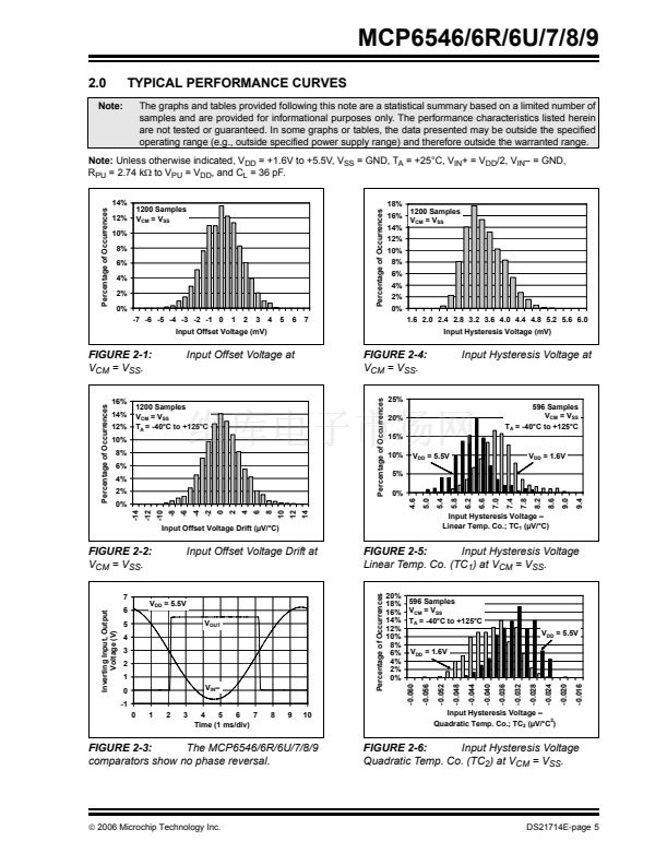
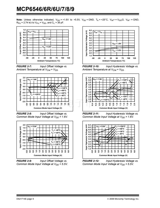
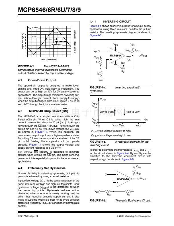
The input offset voltage is the center of the input-referred trip points. The input hysteresis is the difference between the
input-referred trip points.
V
HYST
at differential temperatures is estimated using: V
HYST
(T
A
) = V
HYST
+ (T
A
-25擄C) TC
1
+ (T
A
- 25擄C)
2
TC
2
.
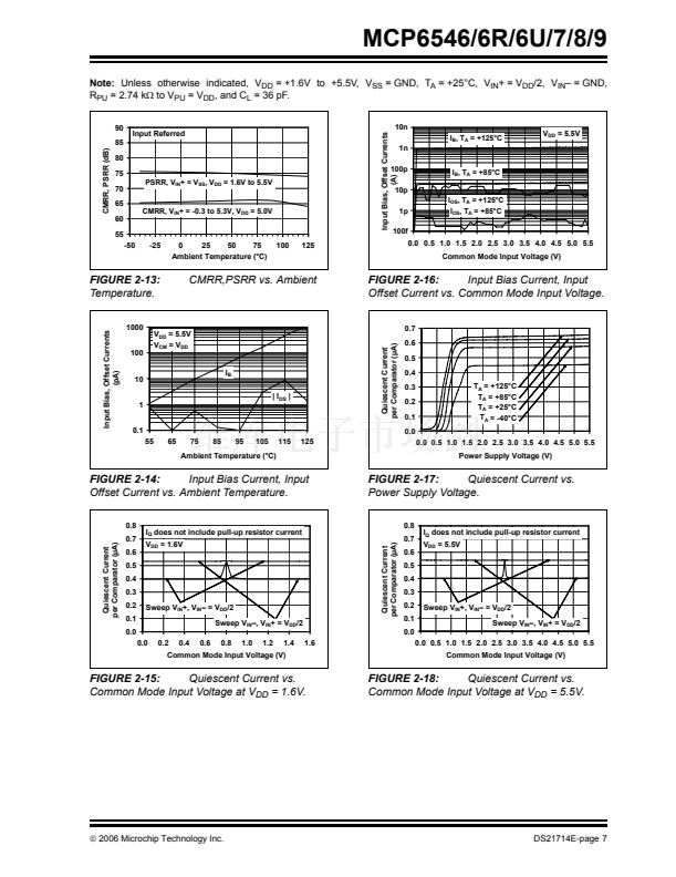
Input bias current at temperature is not tested for the SC-70-5 package
Do not short the output above V
SS
+ 10V. Limit the output current to Absolute Maximum Rating of 30 mA. The minimum
V
PU
test limit was V
DD
before Dec. 2004 (week code 52).
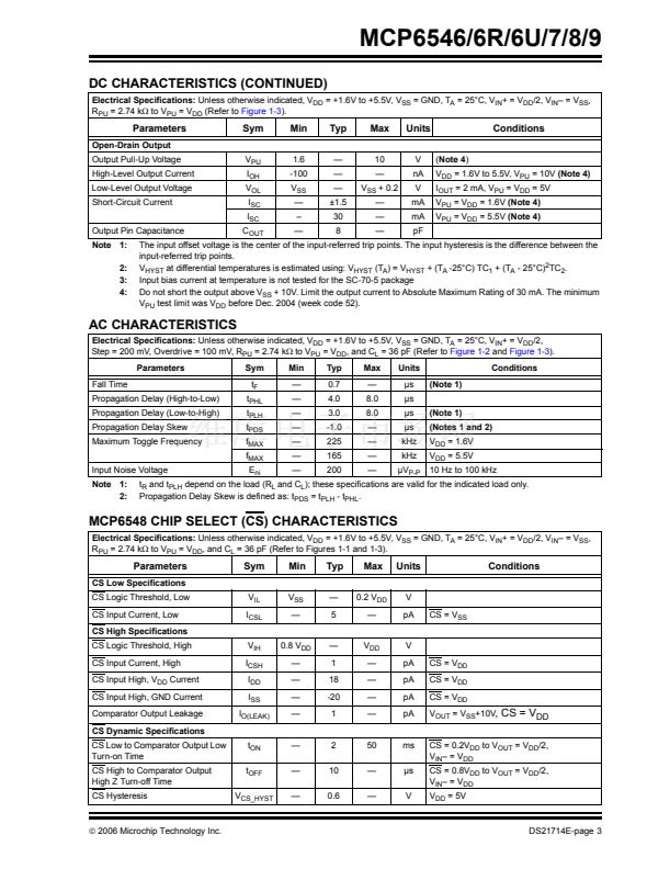
AC CHARACTERISTICS
Electrical Specifications:
Unless otherwise indicated, V
DD
= +1.6V to +5.5V, V
SS
= GND, T
A
= 25擄C, V
IN
+ = V
DD
/2,
Step = 200 mV, Overdrive = 100 mV, R
PU
= 2.74 k惟 to V
PU
= V
DD
, and C
L
= 36 pF (Refer to
Figure 1-2
and
Figure 1-3).
Parameters
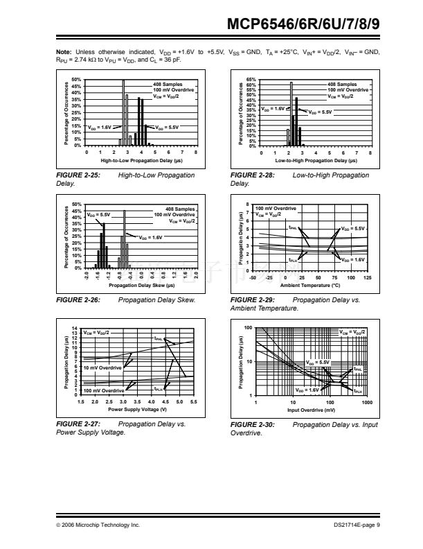
Fall Time
Propagation Delay (High-to-Low)
Propagation Delay (Low-to-High)
Propagation Delay Skew
Maximum Toggle Frequency
Input Noise Voltage
Note 1:
2:
Sym
t
F
t
PHL
t
PLH
t
PDS
f
MAX
f
MAX
E
ni
Min
鈥?/div>
鈥?/div>
鈥?/div>
鈥?/div>
鈥?/div>
鈥?/div>
鈥?/div>
Typ
0.7
4.0
3.0
-1.0
225
165
200
Max
鈥?/div>
8.0
8.0
鈥?/div>
鈥?/div>
鈥?/div>
鈥?/div>
Units
碌s
碌s
碌s
碌s
kHz
kHz
碌V
P-P
(Note 1)
(Notes 1 and 2)
V
DD
= 1.6V
V
DD
= 5.5V
10 Hz to 100 kHz
(Note 1)
Conditions
t
R
and t
PLH
depend on the load (R
L
and C
L
); these specifications are valid for the indicated load only.
Propagation Delay Skew is defined as: t
PDS
= t
PLH
- t
PHL
.
MCP6548 CHIP SELECT (CS) CHARACTERISTICS
Electrical Specifications:
Unless otherwise indicated, V
DD
= +1.6V to +5.5V, V
SS
= GND, T
A
= 25擄C, V
IN
+ = V
DD
/2, V
IN
鈥?= V
SS
,
R
PU
= 2.74 k惟 to V
PU
= V
DD
, and C
L
= 36 pF (Refer to Figures 1-1 and 1-3).
Parameters
CS Low Specifications
CS Logic Threshold, Low
CS Input Current, Low
CS High Specifications
CS Logic Threshold, High
CS Input Current, High
CS Input High, V
DD
Current
CS Input High, GND Current
Comparator Output Leakage
CS Dynamic Specifications
CS Low to Comparator Output Low
Turn-on Time
CS High to Comparator Output
High Z Turn-off Time
CS Hysteresis
Sym
V
IL
I
CSL
V
IH
I
CSH
I
DD
I
SS
I
O(LEAK)
t
ON
t
OFF
V
CS_HYST
Min
V
SS
鈥?/div>
0.8 V
DD
鈥?/div>
鈥?/div>
鈥?/div>
鈥?/div>
鈥?/div>
鈥?/div>
鈥?/div>
Typ
鈥?/div>
5
鈥?/div>
1
18
-20
1
2
10
0.6
Max
0.2 V
DD
鈥?/div>
V
DD
鈥?/div>
鈥?/div>
鈥?/div>
鈥?/div>
50
鈥?/div>
鈥?/div>
Units
V
pA
V
pA
pA
pA
pA
ms
碌s
V
CS = V
DD
CS = V
DD
CS = V
DD
CS = V
SS
Conditions
V
OUT
= V
SS
+10V
,
CS = V
DD
CS = 0.2V
DD
to V
OUT
= V
DD
/2,
V
IN
鈥?= V
DD
CS = 0.8V
DD
to V
OUT
= V
DD
/2,
V
IN
鈥?= V
DD
V
DD
= 5V
漏
2006 Microchip Technology Inc.
DS21714E-page 3
MCP6546T-I/LT 產(chǎn)品屬性
Microchip
校驗器 IC
1 Channel
Analog Comparators
Open Drain
4 us
7 mV
1 uA
+ 85 C
SMD/SMT
SC-70-5
Reel
- 40 C
3000
5.5 V
1.6 V
MCP6546T-I/LT相關型號PDF文件下載
-
型號
版本
描述
廠商
下載
-
英文版
2.7V to 6.0V Single Supply CMOS Op Amps
-
英文版
2.7V to 5.5V Single Supply CMOS Op Amps
-
英文版
2.7V to 6.0V Single Supply CMOS Op Amps
-
英文版
2.7V to 5.5V Single Supply CMOS Op Amps
-
英文版
2.7V to 6.0V Single Supply CMOS Op Amps
-
英文版
2.7V to 5.5V Single Supply CMOS Op Amps
-
英文版
2.7V to 6.0V Single Supply CMOS Op Amps
-
英文版
2.7V to 5.5V Single Supply CMOS Op Amps
-
英文版
2.5V to 5.5V Micropower CMOS Op Amps
-
英文版
2.5V to 5.5V Micropower CMOS Op Amps
-
英文版
2.5V to 6.0V Micropower CMOS Op Amp
-
英文版
2.5V to 5.5V Micropower CMOS Op Amps
-
英文版
2.5V to 6.0V Micropower CMOS Op Amp
-
英文版
2.5V to 5.5V Micropower CMOS Op Amps
-
英文版
2.3V to 5.5V Micropower Bi-CMOS Op Amps
-
英文版
2.3V to 5.5V Micropower Bi-CMOS Op Amps
-
英文版
2.3V to 5.5V Micropower Bi-CMOS Op Amps
-
英文版
2.3V to 5.5V Micropower Bi-CMOS Op Amps
-
英文版
2.3V to 5.5V Micropower Bi-CMOS Op Amps
-
英文版
2.3V to 5.5V Micropower Bi-CMOS Op Amps


 1
1
 2
2
 3
3
 4
4
 5
5
 6
6
 7
7
 8
8
 9
9
 10
10
 11
11
 12
12
 13
13
 14
14
 15
15
 16
16
 17
17
 18
18
 19
19
 20
20
 21
21
 22
22
 23
23
 24
24
 25
25
 26
26
 27
27
 28
28
 29
29
 30
30
 31
31
 32
32
